SOLTEK SL-65F+ User manual

This User‘s Guide & Technical Reference is for assisting system
manufacturers and end-users in setting up and installing the
mainboard.
Everyefforthasbeenmadetoensurethattheinformationinthismanual
is accurate. Soltek Computer Inc. is not responsible for printing or
clericalerrors.Informationinthisdocumentissubjecttochangewith-
outnoticeanddoesnotrepresentacommitmentonthepartofSoltek
ComputerInc.
No part of this manual may be reproduced, transmitted, translated
into any language in any form or by any means, electronic or
mechanical, including photocopying and recording, for any purpose
without the express written permission of Soltek Computer Inc.
Companies and products mentioned in this manual are for identifica-
tion purpose only. Product names appearing in this manual may or
may not be registered trademarks or copyrights of their respective
companies.
Soltek computer inc. Provides this manual “As is “ without war
ranty of any kind, either express or implied, including but not lim-
ited to the implied warranties or conditions of merchantability or fit-
ness for a particular purpose. In no event shall Soltek computer inc.
Be liable for any loss or profits, loss of business, loss of use or data,
interruption of business, or for indirect, special, incidental, or conse-
quentialdamages of any kind, evenif Soltek computer inc. Hasbeen
advised of the possibility of such damages arising from any defect or
error in this manual or product.
© Copyright 2000 Soltek Computer Inc.
All rights reserved.
http://www.soltek.com.tw
e-mail:[email protected]
Model : SL-65F+
Edition : March 2000
Version : 2.0
R

65F+
2
CONTENT
FEATURES ............................................................................... 4
JUMPER SETTING .................................................................. 9
STANDARD CMOS SETUP.................................................... 13
BIOS FEATURES SETUP ...................................................... 15
CHIPSET FEATURES SETUP ............................................... 19
POWER MANAGEMENT SETUP........................................... 23
PnP/PCI CONFIGURATION SETUP ...................................... 27
LOAD SETUP DEFAULTS ..................................................... 29
INTEGRATED PERIPHERALS............................................... 30
SUPERVISOR/USER PASSWORD........................................ 34
IDE HDD AUTO DETECTION ................................................ 35
SAVE & EXIT SETUP............................................................. 35
EXIT WITHOUT SAVING........................................................ 35
Appendix A
Flash Memory Update Installation ....................................... 36
Appendix B
Driver installation .................................................................. 37

65F+
4
SL-65F+
INTEL 82440ZX SOCKET-370
3x 3.3V DIMM sockets.
8MB to 256MB DRAM size.
SYSTEM MEMORY
2x Ultra ATA/33 Bus Master IDE ports.
2x USB ports.
1x PS/2 mouse connector and 1x PS/2 keyboard connector.
1x 2.88MB Floppy port, 2x High Speed 16550A UART ports
and 1x IrDA TX / RX Header.
ONBOARD I/O
ATX power supply connector.
Power-On by LAN(WOL), RTC Alarm, Modem Ring.
POWER
2MB FLASH BIOS.
Licensed AWARD BIOS, supports SCSI / ZIP / LS-120 / CD-
ROM boot and ACPI Power Management.
BIOS
1x AGP slot supports 1x / 2x mode bus; 3x PCI Bus Master
slots; 1x PCI Slave slot; 2x ISA slots.
SLOT
ATX, 4 layers PCB, 17.0cm x 30.5cm size.
FORM FACTOR / PCB
F E A T U R E
CHIPSET
Intel 82440ZX chipset.
Supports Intel PPGA Celeron 370 CPUs 300 ~ 533MHz or
higher.
Supports Intel FC-PGA Pentium III (Coppermine) CPUs 500E
~ 750 MHz or higher.
Supports Cyrix Joshua CPUs.
Supports 66/ 75*/ 83*/ 100/ 103*/ 112*/ 124*/ 133*/ 140*/
150*MHz system bus speeds.
Clock multipliers up to 8x.
PROCESSOR

5
65F+
Default setting: Intel Celeron 300A/66MHz.
NOTE: For 100MHz/133MHz CPU environment, the SDRAM sepc must comply
with PC-100/PC-133 spec.
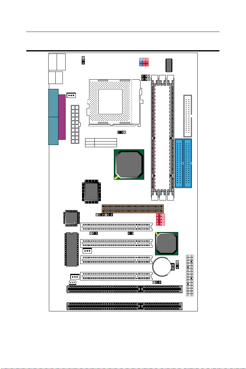
M O T H E R B O A R D D I A G R A M
1 3
1 3
1 1 1 3
1 3
1 3
1 3
JP12
JP13
JP14
JP15
1 3
1 3
JP21
JP22
1 3
1 3
JP3
JP4
JP5
JP16
JP11JP10
1 3
JVGA1
JP20
1 3
JP17
3
1
JBAT1
3
1
JP2
FAN2
FAN1
FAN3
SPK RST PWR/LED SUSLED
HD/LED IR PWR SUSPEND
J2
J3
15
15
JWOL1
AGP
PCI 1
PCI 2
PCI 3
PCI 4 Slave PCI)
FDC
DIMM1
DIMM2
DIMM3
IDE2
IDE1
SOCKET 370
ATX POWER
ISA1
ISA2
FLASH BIOS
Li
Battery
Clock
Generator
LPT1
COM2 COM1 PS/2
MOUSE
PS/2
K/B
upper
lower
USB1
USB0
upper
lower
ES1938S
I/O
Controller
Intel
Cyrix
1-2 SHORT
JP20/JP21/JP22
2-3 SHORT
Intel
82440ZX
Intel
82371
PIIX4
Please refer to next page for the precise
arrangement of DIMM module.

65F+
6
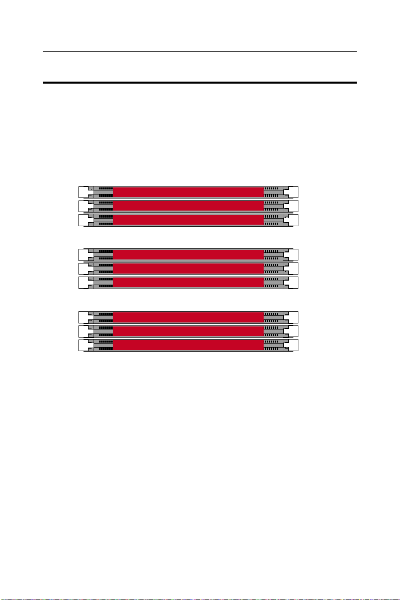
The 82440ZX motherboard supports 168 pins DIMM of 4MB, 8MB,
16MB, 32MB, 64MB, 128MB and 256MB to form a memory sie between
8MB to 256MB(SDRAM).
82440ZX chipset provides “Table-Free” function, but do remember
that the DRAM must be 3.3V Unbuffered and 4 clock type. User can
use two DIMMs without any limit but if uses three DIMMs then must
follow the rules below:
NOTE: ONLY SINGLE SIDE SDRAM CAN BE PLUGGED WHEN DIMM2/DIMM3
SIMULTANEOUSLY USED.
SYSTEM MEMORY CONFIGURATION
DIMM1
DIMM2
DIMM3
Double or single side SDRAM
EMPTY
A.
DIMM1
DIMM2
DIMM3
Double or single side SDRAM
Single side SDRAM
Single side SDRAM
B.
DIMM1
DIMM2
DIMM3
Double or single side SDRAM
EMPTY
Double or single side SDRAM
C.

7
65F+
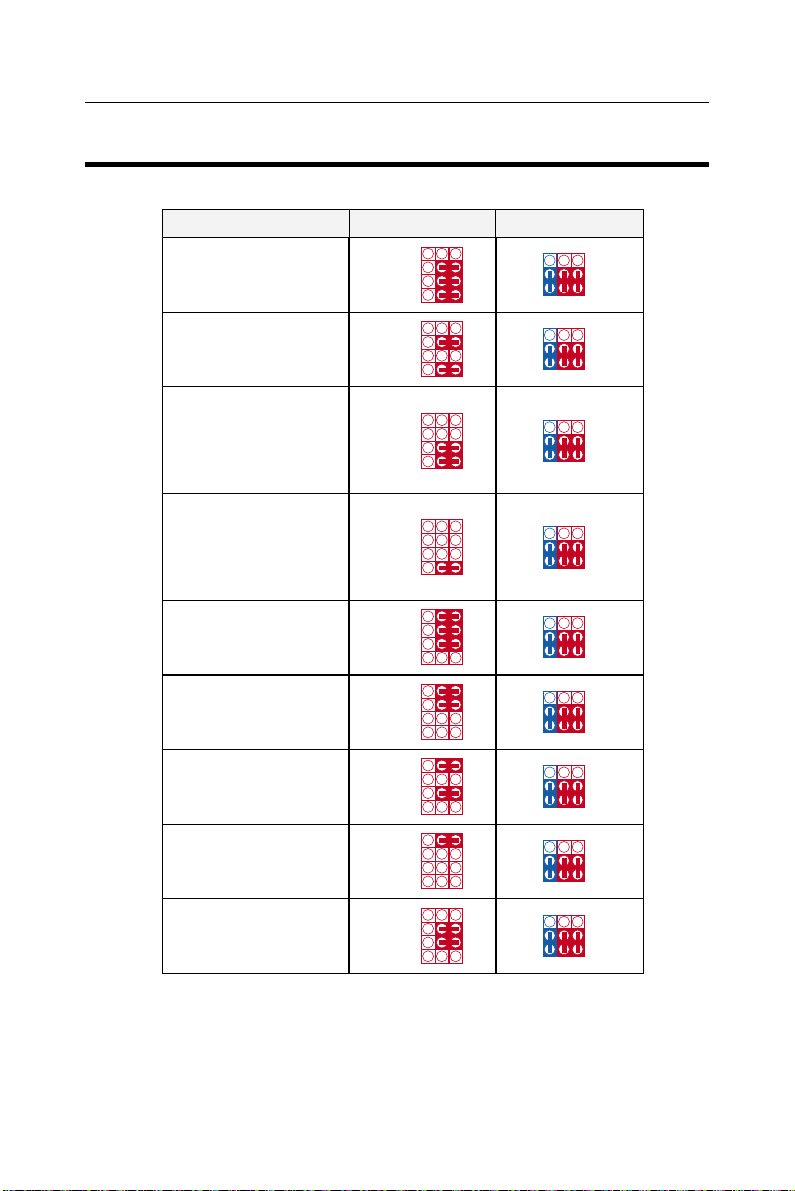
C P U C L O C K S E T T I N G
CPU Type Configuration
CPU MODEL BUS RATIO BUS CLOCK
NOTE: #) Pentium III Coppermin FC-PGA CPUs.
Celeron 300/66
66MHz * 4.5x)
Pentium III 600EB/133
#
133MHz * 4.5x)
JP12
JP13
JP14
JP15
1 3
1 3
1 3
1 3
1 3
1 3
1 3
JP3
JP4
JP5
Pentium III 533EB/133
#
133MHz * 4.0x)
JP12
JP13
JP14
JP15
1 3
1 3
1 3
1 3
1 3
1 3
1 3
JP3
JP4
JP5
Celeron 333/66
66MHz * 5.0x)
Pentium III 500E/100
#
100MHz * 5.0x)
Pentium III 667B/133
#
133MHz * 5.0x)
JP12
JP13
JP14
JP15
1 3
1 3
1 3
1 3
1 3
1 3
1 3
JP3
JP4
JP5
Celeron 366/66
66MHz * 5.5x)
Pentium III 550E/100
#
100MHz * 5.5x)
Pentium III 733B/133
#
133MHz * 5.5x)
JP12
JP13
JP14
JP15
1 3
1 3
1 3
1 3
1 3
1 3
1 3
JP3
JP4
JP5
Celeron 400/66
66MHz * 6.0x)
Pentium III 600E/100
#
100MHz * 6.0x)
JP12
JP13
JP14
JP15
1 3
1 3
1 3
1 3
1 3
1 3
1 3
JP3
JP4
JP5
Celeron 433/66
66MHz * 6.5x)
Pentium III 650/100
#
100MHz * 6.5x)
JP12
JP13
JP14
JP15
1 3
1 3
1 3
1 3
1 3
1 3
1 3
JP3
JP4
JP5
Celeron 466/66
66MHz * 7.0x)
Pentium III 700/100
#
100MHz * 7.0x)
JP12
JP13
JP14
JP15
1 3
1 3
1 3
1 3
1 3
1 3
1 3
JP3
JP4
JP5
Celeron 500/66
66MHz * 7.5x)
Pentium III 750/100
#
100MHz * 7.5x)
JP12
JP13
JP14
JP15
1 3
1 3
1 3
1 3
1 3
1 3
1 3
JP3
JP4
JP5
Celeron 533/66
66MHz * 8.0x)
JP12
JP13
JP14
JP15
1 3
1 3
1 3
1 3
1 3
1 3
1 3
JP3
JP4
JP5

65F+
8
J U M P E R S E T T I N G
FAN# FUNCTION
FAN1 CPU FAN
FAN2 POWER FAN
FAN3 CHASSIS FAN
FAN#: Onboard FAN (12V) Connector
Keyboard Power On JP2
JP2: Keyboard Power On
Disabled (default) 1 3
Enabled 1 3
NOTE 1: If motherboard does not support keyboard power on function, the JP2
will be fixed by jumperwire.
NOTE 2: When the keyboard power on function shows any compatible problem,
choose Disabled and report the keyboard model to your vender/maker.
NOTE 3: Keyboard power on function must be set from the BIOS. Refer to the
“Integrated Peripherals” sector.
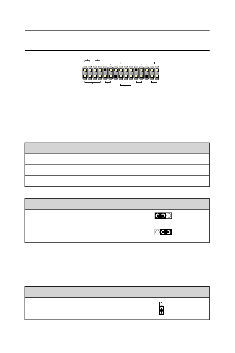
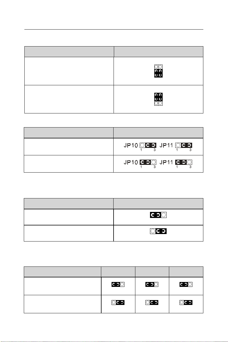
Signal Level Shift Control JP3
JP3: Signal Level Shift Control
Factory default setting
(default) 3
1
1
1
15
15
EF G
C
H I
D
A1 A2 B
J2
J3
++
--
+-
A1: 1st HDD LED
B. : INFRARED (IR)
D. : SUSPEND CONNECTOR
F. : RESET SWITCH
H. : KEYLOCK
A2: 2nd HDD LED
C. : POWER SWITCH
E. : SPEAKER
G. : POWER LED
I. : SUSPEND LED

9
65F+
JP10 / JP11: USB Port Select JP10 / JP11USB Port
Redirect USB port1 to USB
connector (default)
Redirect USB port1 to AGP
JP4 / JP5: CPU Host Clock Select JP4 / JP5
CPU Host Clock
Auto (default) 3
1
3
1
JP4 JP5
100MHz (overlock) 3
1
3
1
JP4 JP5
JP17: Power Lost Resume
This jumper allows user to use the switch of ATX power supply to control ON/
OFF switch directly instead of using the power switch on the motherboard.
NOTE: This feature must work with BIOS. Please refer to the BIOS “Power On
After PWR-Fail” sector.
Power Lost Resume JP17
Enabled 1 3
Normal (default) 1 3
JP20 / JP21 / JP22: Intel / Cyrix CPU Select
CPU TYPE
Intel CPU (Default)
Cyrix Joshua CPU
JP22
1 3
1 3
JP21
1 3
1 3
JP20
1 3
1 3

65F+
10
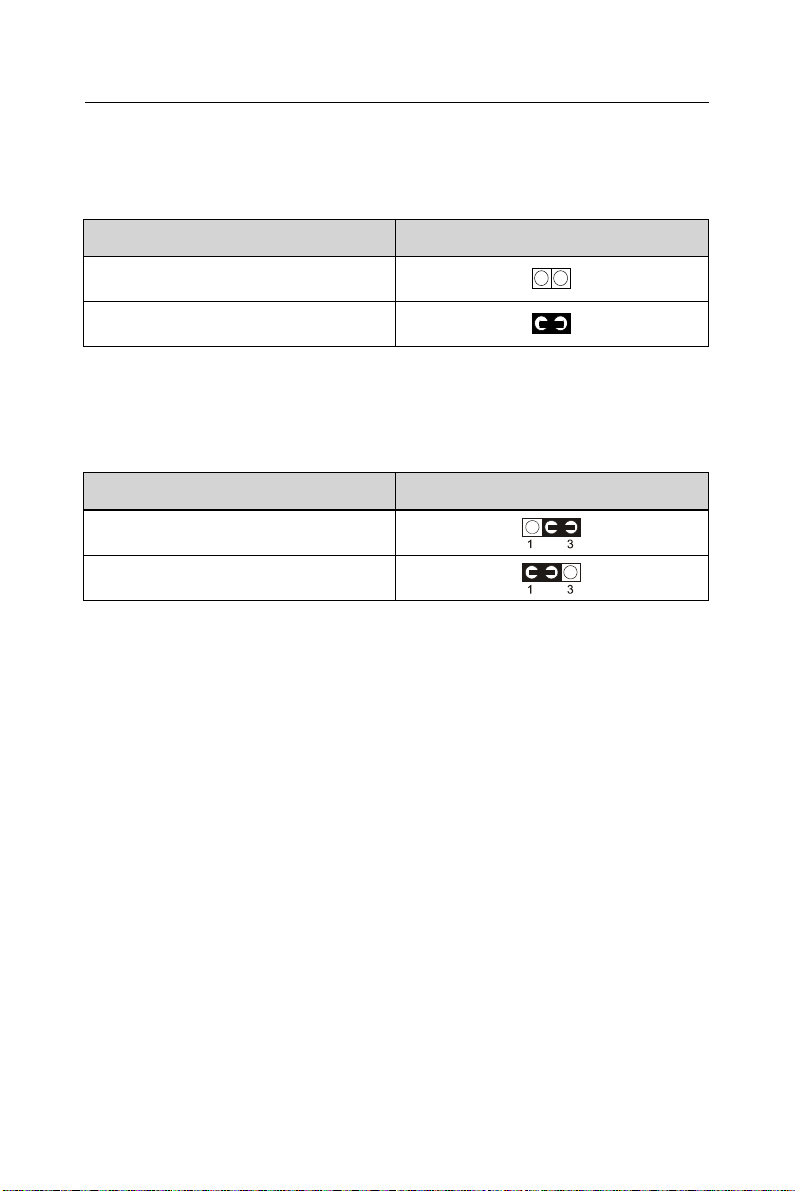
JBAT1: Clear CMOS data
Clear the CMOS memory by shorting this jumper 2 & 3 momentarily, and then
remove the cap back to 1 & 2 to retain original CMOS setting.
JBAT1
Clear CMOS Data
Retain Data (default)
JBAT1
JVGA1: VGA Use
This jumper is set for the PCI VGA card only. Open this jumper when the system
is not able to boot up. If you use AGP card, it is important to set default with
JVGA1. JVGA1
For PCI VGA card
Normal (default)
JWOL1: Wake On LAN (WOL) Connector
This jumper is designed to use LAN to boot up the system. Connect the wake
on signal from LAN card to this connector.
***For support WOL, the ATX power supply has to have at least 5V/720mA
standby current.***
Table of contents
Other SOLTEK Motherboard manuals

SOLTEK
SOLTEK SL-65DVB User manual

SOLTEK
SOLTEK SL-85DR User manual

SOLTEK
SOLTEK SL-53A2 Use and care manual

SOLTEK
SOLTEK SL-65FVB User manual

SOLTEK
SOLTEK SL-55B5 User manual

SOLTEK
SOLTEK SL-85DIV User manual

SOLTEK
SOLTEK 85DRV5 User manual

SOLTEK
SOLTEK 86SP3 User manual

SOLTEK
SOLTEK SL-65ME User manual

SOLTEK
SOLTEK SL-PM800I-R User manual

SOLTEK
SOLTEK SL-67EZ Use and care manual

SOLTEK
SOLTEK KT400 User manual

SOLTEK
SOLTEK NF4-754RL User manual

SOLTEK
SOLTEK SL-55D5 Use and care manual

SOLTEK
SOLTEK SL-67EB Plus User manual

SOLTEK
SOLTEK SL-56D1 User manual

SOLTEK
SOLTEK 85MR3 User manual

SOLTEK
SOLTEK SL-67B-W User manual

SOLTEK
SOLTEK SL-65KIV User manual

SOLTEK
SOLTEK SL-865G3 User manual