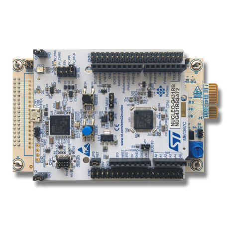
SOLTEK SL-56D1 User manual

i
Notice to End Users
This UserÕs Guide & Technical Reference is for assisting system
manufacturers and end users in setting up and installing the
mainboard.
Every effort has been made to ensure that the information in this
manual is accurate. Soltek Computer Inc. is not responsible for
printing or clerical errors. Information in this document is subject
to change without notice and does not represent a commitment on
the part of Soltek Computer Inc.
No part of this manual may be reproduced, transmitted, translated
into any language in any form or by any means, electronic or
mechanical, including photocopying and recording, for any purpose
without the express written permission of Soltek Computer Inc.
Companies and products mentioned in this manual are for
identification purposes only. Product names appearing in this
manual may or may not be registered trademarks or copyrights of
their respective companies.
SOLTEK COMPUTER INC. PROVIDES THIS MANUAL ÒAS ISÓ
WITHOUT WARRANTY OF ANY KIND, EITHER EXPRESS OR IMPLIED,
INCLUDING BUT NOT LIMITED TO THE IMPLIED WARRANTIES OR
CONDITIONS OF MERCHANTABILITY OR FITNESS FOR A
PARTICULAR PURPOSE. IN NO EVENT SHALL SOLTEK COMPUTER
INC. BE LIABLE FOR ANY LOSS OR PROFITS, LOSS OF BUSINESS, LOSS
OF USE OR DATA, INTERRUPTION OF BUSINESS, OR FOR INDIRECT,
SPECIAL, INCIDENTAL, OR CONSEQUENTIAL DAMAGES OF ANY
KIND, EVEN IF SOLTEK COMPUTER INC. HAS BEEN ADVISED OF THE
POSSIBILITY OF SUCH DAMAGES ARISING FROM ANY DEFECT OR
ERROR IN THIS MANUAL OR PRODUCT.
© Copyright 1998 Soltek Computer Inc. All right reserved
Web site: http://www.soltek.com.tw
email: [email protected]
Edition: August 1998
Version: 1.0
SL-56D5/D1 SERIALS
®

ii
Contents
Chapter 1: Introduction --------------------------------------- 1
Features -------------------------------------------------------------------------1
CPU ------------------------------------------------------------------------1
Chipset -------------------------------------------------------------------- 1
L2 Cache ------------------------------------------------------------------1
Main Memory ----------------------------------------------------------- 1
BIOS ------------------------------------------------------------------------ 2
I/O Function -------------------------------------------------------------2
Other Functions --------------------------------------------------------- 2
Mainboard Setting for Pentium MMX-200----------------------------- 3
Chapter 2: Hardware Setup---------------------------------- 5
CPU VCORE Voltage Setting---------------------------------------------- 5
JP4: CPU VCore Voltage Setting -----------------------------------5
AGP Driver for Win95 Installation --------------------------------------6
Requirement -------------------------------------------------------------6
Installation Procedure -------------------------------------------------6
Intel Pentium MMXÐ166/200/233 CPUs ------------------------------7
AMD K6 CPU Settings------------------------------------------------------8
AMD K6 Ð 166/200/233 CPUs and K6-2 266 CPU ------------- 8
AMD K6-2 Ð 250/266/300/333/350 CPU Settings ------------------9
Cyrix MII Ð PR300/333/350 CPUs------------------------------------- 10
IDT C6 Ð 200/225/240 CPUs -------------------------------------------- 11
Intel Pentium/AMD K5 Ð 133/166/200 CPUs---------------------- 12
System Memory Configuration----------------------------------------- 13
Jumper Settings ------------------------------------------------------------- 13
JP8: Clear CMOS Data ---------------------------------------------- 13
JP11, JP12: CPU Dual/Single Voltage Select ------------------ 14
SW1: 4~6: Bus Ratio Select----------------------------------------- 14
JP6, JP7: Chipset Clock Settings ---------------------------------- 15

Contents iii
IDE LED Activity Light: (J1 pin1Ð4)------------------------------ 15
Infrared Port Module Connector (J1 pin6Ð10) ----------------- 15
J1 pin12, 13: ATX Power Button ---------------------------------- 15
J1 pin14, 15: Reserved ----------------------------------------------- 15
Speaker Connector (J2 pin1Ð4) ------------------------------------ 15
Reset Switch (J2 pin5, 6)--------------------------------------------- 16
Power LED and Keylock Switch (J2 pin8Ð12)------------------ 16
JWOL1: Wake On Lan (WOL) Connector ---------------------- 16
Turbo LED (J2 pin14, 15)-------------------------------------------- 17
J1 Switch Signal Summary ----------------------------------------- 18
J2 Switch Signal Summary ----------------------------------------- 19
Chapter 3: BIOS Setup ---------------------------------------20
Standard CMOS Setup ---------------------------------------------------- 21
BIOS Features Setup ------------------------------------------------------- 23
Chipset Features Setup --------------------------------------------------- 26
Power Management Setup ----------------------------------------------- 29
PnP/PCI Configuration Setup ------------------------------------------ 31
Load Setup Defaults ------------------------------------------------------- 34
Integrated Peripherals ---------------------------------------------------- 35
Supervisor/User Password---------------------------------------------- 38
IDE HDD Auto Detection ------------------------------------------------ 39
Save & Exit Setup ---------------------------------------------------------- 39
HDD Low Level Format -------------------------------------------------- 39
Exit Without Saving ------------------------------------------------------- 40


Introduction 1
Chapter 1
Introduction
Features
CPU
1. Supports Intel Pentium MMX CPUs at 100 ~ 233 MHz;
2. Supports Cyrix 6x86(L) CPUs at PR133+~ PR200+MHz
and 6x86MX (MII) CPUs at PR166+~ PR350+MHz;
3. Supports AMD K5: PR100 ~ PR200MHz, AMD K6: 166 ~
333MHz, and AMD K6-2: 250 ~ 350MHz;
4. Suports IDT C6: 200 ~ 225MHz;
5. Provides SOCKET 7 ZIF Socket;
6. Supports 66/75/83/95/100/112/124/133 MHz CPU clock.
Chipset
1. VIA Apollo MVP3 chipset;
2. PCI Rev 2.1 and APM1.1/1.2 compliant.
L2 Cache
1. Onboard supports 512K/1MB write back cache with
Pipelined Burst SRAMs.
Main Memory
1. Memory range from 4MB (minimum) to 768MB
(maximum) with DRAM Table Free configurations;
2. Supports SDRAM with 8/10ns;
3. Supports 3 pcs of 168pin DIMM sockets (3.3V
unbuffered 4 clock type).

2
BIOS
1. AWARD Plug and Play BIOS;
2. Supports Advanced Power Management, ACPI
Function;
3. Flash Memory for easy upgrade.
I/O Function
1. Integrated USB (Universal Serial Bus) controller with
two USB ports;
2. Supports 2 IDE channels with 4IDE devices (including
120MB IDE floppy);
3. Provides PCI IDE Bus Master function;
4. One floppy port;
5. Two high speed 16550 FIFO UART ports;
6. One parallel port with EPP/ECP/SPP capabilities;
7. PS/2 mouse connector;
8. Infrared module connector.
Other Functions
1. ATX Form Factor with 18cm x 30.5cm;
2. 5 PCI Master slots, 2 ISA slots, and 1 AGP slot;
3. Supports SCSI/CD-ROM Boot function;
4. Supports Wake On Lan (WOL)*, Modem Ring Up
function.
Note: 1. Make sure that the SDRAM module not only has
to be 168 pin DIMM but designed for 3.3V
unbuffered SDRAM as well. Double check with
the SDRAM supplier before install any
SDRAMs. The mainboard manufacturer has no
obligation to any damage of the board by using
the incorrect specification of SDRAM.
2. For 100MHz CPU environment, the SDRAM
must compliant PC-100MHz specification,
otherwise, the system maybe unstable.
*: To support WOL, the ATX Power Supply has to have
at least 5V/720mA standby current.

Introduction 3
Mainboard Setting for Pentium MMX-200
The default settings of the following figure is for the INTEL
Pentium MMX-200, Vcore: 2.8V.
ISA2
PCI5
FLASH BIOS
ISA1
PCI4
PCI3
PCI2
PCI1
AGP
VT82C586B
JP8
1
J1
J2
SPK KEYLOCK T/LED
HD LED IR CON PWR
RESET
JWOL1
Li BAT
W83877F
/877AF
VIA
MVP3
Chipset
Pipelined
SRAM Pipelined
SRAM
FDD1
IDE2
IDE1
JP6
JP7
1
TAG RAM
MMX-200 CPU
DIMM3
DIMM2
DIMM1
Clock Gen.
FAN1
JP4
1
ATX Power Conn.
LPT1
COM2 COM1
USB0
USB1
PS/2
K/B
Upper
Lower
654321
ON
SW1
Off
On
On
On
Off
Off
JP12
JP11
1
Figure 1–1. Motherboard Layout
Note: Double Check JP6/JP7 if system can not be boot up.

Chapter 2
Hardware Setup
CPU V
CORE
Voltage Setting
JP4, JP11, JP12: CPU V
Core
Voltage Setting
11
11
V
Core
Voltage
2.2V
K6-266
(or higher)
K6-2
JP4
JP12
JP11
JP4
JP12
JP11 JP4
JP12
JP11 JP4
JP12
JP11
JP4
JP12
JP11 JP4
JP12
JP11
1
V
Core
Voltage
2.8V
MMX, 6x86L
V
Core
Voltage
2.9V
K6-166/200
6x86MX/MII
V
Core
Voltage
3.2V
K6-233
1
V
Core
Voltage
3.3V
IDT C6
V
Core
Voltage
3.5V
Pentium (P54C)
6x86
K5
1
JP12
JP11
1
JP12
JP11
1
1
JP12
JP11
1
JP12
JP11
1
JP12
JP11
1
JP12
JP11
CPU Type VCore
Pentium, 6x86, K5 3.52V
MMX, 6x86L 2.8V
IDT C6 3.3V
K6-166/200, 6x86MX (MII) 2.9V
K6-233 3.2V
K6-266 (or higher), K6-2 2.2V

6
Note: 1. Refer to the table above to choose the correct
voltage for the CPU everytime that you install a
CPU.
2. Make sure that your JP4 is matched with the
CPU voltage, otherwise will damage the CPU or
make the system unstable.
3. When the new CPU is announced and is not
listed on this manual, please refer to the above
table, select the correct voltage setting for it.
AGP Driver for Win95 Installation
Requirement
¥ Microsoft Windows95OSR2.1 (OSR2.0 with USB upgrade)
¥ Apollo MVP3 AGP VxD Driver
¥ AGP VGA Card with Driver
¥ DirectX 5.0 DDK (or higher) or SDK
Installation Procedure
Step1 Go to the next step if you are running
Win95OSR2.0/2.1, and if not, install Windows95
4.00.950B or later version
Step2 Install USBSUPP.EXE program (USB upgrade)
Step3 Install Microsoft DirectX 5.0 (or higher) DDK or
SDK
Step4 Install AGP driver for Windows95
Step5 Install Apollo MVP3 AGP VxD Driver, run
ÒSETUP.EXEÓ program
To make sure if the Apollo MVP3 AGP driver is properly
installed, boot up the system and run the ÒRegeditÓ to check
if the following path with VIAGARTD exists:

Hardware Installation 7
ÒHKEY_LOCAL_MACHINES\System\CurrentControlSet\
Services\VxDÓ.
Follow the below procedure to check if the AGP driver is
capable to activate:
1. Activate ÒControl Panel,Ó
2. Click ÒDirectX,Ó
3. Click ÒDirectDraw,Ó and
4. Check if there are some values in ÒBitÓ and ÒOverlays.Ó
If there are some values, the AGP is able to activate.
Intel Pentium MMX–166/200/233 CPUs
MMX-200 CPU
JP4
1
SW1
1
Off
2
On
3
On
4
On
On
56 123456 123456
Off
ON ON ON
MMX–166
Off
On
On
On
On
On
Off
Off
MMX–200
Off
Off
Off
Off
MMX–233
(2.8V)
JP6
JP7
1
JP12
JP11
1
Figure 2–1. CPU Type Configuration
This manual suits for next models
1
Table of contents
Other SOLTEK Motherboard manuals

SOLTEK
SOLTEK SL-845GVI User manual

SOLTEK
SOLTEK SL-67G60 Use and care manual

SOLTEK
SOLTEK SL-75KV User manual

SOLTEK
SOLTEK SL-65EB User manual

SOLTEK
SOLTEK 85DRV5-L User manual

SOLTEK
SOLTEK SL-65MIE User manual

SOLTEK
SOLTEK SL-55F5 User manual

SOLTEK
SOLTEK 85ERV User manual

SOLTEK
SOLTEK 75DRV User manual

SOLTEK
SOLTEK SL-65LIV-T User manual

SOLTEK
SOLTEK SL-85LIR User manual

SOLTEK
SOLTEK SL-PM800I User manual

SOLTEK
SOLTEK SL-67D User manual

SOLTEK
SOLTEK B9A-FGR User manual

SOLTEK
SOLTEK SL-85SID User manual

SOLTEK
SOLTEK SL-56H5 User manual

SOLTEK
SOLTEK KT400-C User manual

SOLTEK
SOLTEK SL-75KAV User manual

SOLTEK
SOLTEK SL-75MIV User manual

SOLTEK
SOLTEK SL-53D2 Use and care manual