ST STEVAL-SMARTAG2 User manual

Introduction
The STEVAL-SMARTAG2 is an NFC-enabled sensor node, which embeds inertial MEMS sensors and environmental sensors,
an STM32 microcontroller, and a dynamic NFC tag for communication with NFC readers, such as tablets and smartphones.
The STEVAL-SMARTAG2 can optionally be equipped with a battery charger fed through a full-wave rectifier for NFC energy
harvesting (to be put on top of the energy harvester already embedded in the dynamic NFC tag), a secure element to support
authentication and state-of-the-art cryptographic security, and a real-time clock (RTC) with an embedded crystal oscillator to
enable an accurate timekeeping and time stamping.
The board has a small and thin form factor, comparable to the size of a credit card. This makes it particularly fit for deployment
in the field and data collection.
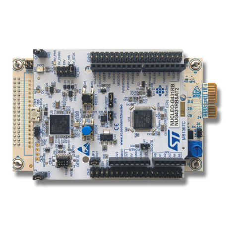
Figure 1. STEVAL-SMARTAG2 evaluation board (top and bottom views)
Getting started with the STEVAL-SMARTAG2 NFC dynamic tag sensor and
processing node evaluation board
UM3034
User manual
UM3034 - Rev 1 - October 2022
For further information contact your local STMicroelectronics sales office. www.st.com

1Getting started
1.1 Safety operating use and conditions
Any use of this device not specified by the manufacturer might compromise the protection mechanisms that come
with the device.
•All components, with few exceptions, have an operating temperature range from -40 to +85°C. Some
components, such as the STM32L4P5CG microcontroller and the ST25DV64KC NFC EEPROM, have
options with an operating range up to +125°C (but the RF interface only works up to +105°C).
• Operating ambient pressure ranges from 260 to 1260 hPa. All sensors might be sensitive to extreme
changes in the ambient pressure.
• Operating ambient relative humidity ranges from 0 to 100%. The board is not protected against water
condensation. A suitable water-resistant coating should be applied to the board and its components. Any
difference in the thermal expansion coefficient creates a mechanical stress between the PCB and the plastic
package of the components. This might affect all on-board sensors. When a coating is applied, the venting
hole in the package of LPS22DF should be covered to avoid contaminating the sensing element.
Note: The battery limits the temperature, humidity, and ambient pressure operating range. Depending on their
chemistry, typical batteries have a very limited or no functionality at or below 0°C. Moreover, rechargeable
batteries cannot operate above +45°C. Select a suitable energy source for the operation at low and high
temperatures, ambient pressure, or relative humidity.
Operating conditions for normal operation
• Temperature between -40 and +85°C. Take care to ensure the battery performance below 0°C and above
45°C.
• Ambient pressure between 260 and 1260 hPa. Extreme values or fast variations might cause mechanical
stress in the sensor packages and affect measurement accuracy.
• Relative humidity between 0 and 100%. The board is not protected against condensation of water.
• FCC part 15 subpart C verification conditions: indoor environment, temperature up to 45°C, humidity range
between 20% and 80%.
ST25DVKC NFC EEPROM
• Operating conditions: temperature -40 to +85°C, other packages, and device grades are available.
• Absolute maximum ratings: voltage -0.5 to 6.5V, 11V between RF input pins and -0.5 to 5.5V between RF
and supply pin, storage temperature -65 to 150°C.
Note: When the harvesting is active, the RF communication is not guaranteed. The harvesting output is not used if
the battery is present and if it has a higher voltage due to the diode-or configuration. A mismatch in the form
factors of NFC antennas might reduce the harvester output and compromise the RF communication. For further
information, refer to AN4913.
STM32L4P5CG MCU
• Operating conditions: temperature -40 to +85°C, maximum junction temperature 105°C. Other packages and
device grades are available.
• Absolute maximum ratings: voltage -0.3 to 4 V, -0.3 to 1.4 V for the external SMPS pin, storage temperature
-65 to 150°C, maximum junction temperature +150°C.
Inertial sensors
•LSM6DSO32X
– Operating conditions: temperature -40 to +85°C, acceleration up to 32 g, angular velocity up to 2000
dps.
– Absolute maximum ratings: voltage -0.3 to 4.8 V, storage temperature -40 to +125°C, acceleration
20’000 g for 0.2 ms.
UM3034
Getting started
UM3034 - Rev 1 page 2/38

•LIS2DUXS12
–Operating conditions: temperature -40 to +85°C, acceleration up to 16 g.
– Absolute maximum ratings: voltage -0.3 to 4.3 V, storage temperature -40 to +125°C, acceleration
10’000 g for 0.2 ms, 3000 g for 0.5 ms.
•H3LIS331DL
– Operating conditions: temperature -40 to +85°C, acceleration up to 400 g.
– Absolute maximum ratings: voltage -0.3 to 4.8 V, storage temperature -40 to +125°C, acceleration
10’000 g for 0.2 ms, 3000 g for 0.5 ms.
Ambient/environmental sensors
•LPS22DF
– Operating conditions: temperature -40 to +85°C, ambient pressure 260 to 1260 hPa.
– Absolute maximum ratings: voltage -0.3 to 4.8 V, storage temperature -40 to +125°C, ambient
overpressure 2 MPa.
•STTS22H
– Operating conditions: contact temperature -40 to +125°C.
– Absolute maximum ratings: voltage -0.3 to 4.8 V, storage temperature -40 to +125°C.
•VD6283TX
– Operating conditions: temperature -30 to +85°C.
– Absolute maximum ratings: voltage -0.5 to 2.5 V, storage temperature -40 to +125°C.
STLQ020 voltage regulator
• Operating conditions: temperature -40 to +125°C, input voltage 2 to 5.5 V, short circuit current 380 mA.
• Absolute maximum ratings: voltage -0.3 to 7 V, storage temperature -55 to +150°C, maximum junction
temperature 150°C.
STSAFE-A110 secure element (optional)
• Operating conditions: temperature -40 to +105°C
• Absolute maximum ratings: voltage -0.3 to 7 V, storage temperature -65 to 150°C.
M41T62LC real-time clock with embedded crystal (optional)
• Operating conditions: temperature -40 to +85°C.
• Absolute maximum ratings: voltage -0.3 to 5 V, storage temperature during soldering -55 to +125°C.
STBC15 battery charger (optional)
• Operating conditions: temperature -40 to +85°C, input voltage up to 6.5 V.
• Absolute maximum ratings: voltage -0.3 to 7 V, -0.3 to 5.5 V on battery and system output pin, storage
temperature -65 to +150°C, maximum junction temperature +125°C.
CR2032 or LIR2032 coin cell battery
The battery is not included in the board package. Several device grades are available. Refer to the manufacturer
datasheet.
Note: A typical CR2032 lithium/manganese-dioxide battery has a 220 mAh nominal capacity and 3 V open-circuit
voltage at room temperature. At -20°C, the open-circuit voltage is reduced from 3 V down to 2.2-2.7 V for 1
k-100 kΩ loads. The capacity is reduced from 220 mAh to 45-175 mAh for 1 k-100 kΩ loads. The inability of the
battery to sustain peak currents at low temperatures might prevent the correct system operation.
UM3034
Safety operating use and conditions
UM3034 - Rev 1 page 3/38

1.2 Overview
Figure 2. STEVAL-SMARTAG2 components
Note: Components highlighted in yellow are populated at the factory. Components highlighted in gray are optional.
STEVAL-SMARTAG2 components
•ST25DV64KC-JF6D3 dynamic NFC/RFID tag with a 64-Kbit EEPROM, fast transfer mode capability, and
an operating band of 13.56 MHz (HF). It is a two-wire I²C serial interface (up to 1 MHz), with a contactless
interface based on the ISO/IEC 15693 (all modulations, coding, sub-carrier modes, and data rates). It is NFC
Forum Type 5 tag-certified, with fast read access (up to 53 Kbit/s), single and multiple blocks, read and write.
The RF interface can be enabled/disabled from the I²C host controller. The EEPROM data retention is 40
years. The write cycle endurance is 1 M million at 25 degrees. It features fast data transfer mode between
the I²C and the RF interface, half-duplex 256-byte dedicated buffer. The user memory areas (1-4) can be
protected for read and/or write with three 64-bit passwords in RF and one 64-bit password in I²C. An NFC
energy harvester is embedded.
– The fast data transfer mode with dedicated buffer can be used to transfer a new binary program to the
host microcontroller.
– The energy harvester is connected in diode-OR with the battery output (or the battery charger when it
is present) to power the whole system.
•STM32L4P5CGU6 microcontroller ultra-low power (110 µA/MHz in LDO mode), which belongs to the
STM32L4+ series, based on the ARM Cortex-M4F 32-bit RISC core. Its operating frequency is up to
120 MHz, with a single-precision floating-point unit (FPU), support for digital signal processing (DSP)
instructions, and memory protection unit (MPU). The device embeds 1 Mbyte of flash memory and 340
Kbytes of SRAM, with several protection mechanism (readout and write protection, proprietary code readout
protection, and firewall).
– Two contact pads on the board are connected to specific microcontroller pins to support the anti-
tamper function.
Note: This function is available only when the STSAFE-A110 and the M41T62 are not populated, and the
serial I²C2 bus peripheral is not needed.
UM3034
Overview
UM3034 - Rev 1 page 4/38

• Inertial sensors:
–LSM6DSO32X inertial module (iNEMO) with 6DoF (degrees of freedom): three-axis accelerometer (4,
8, 16, 32 g full-scale) and three-axis gyroscope (125, 250, 500, 1000, 2000 dps full scale). The peak
power consumption is 0.55 mA for the accelerometer and gyroscope in the high-performance mode
at 6.6 kHz output data rate (ODR) and can be reduced down to 4.4 µA for the accelerometer only
in the ultra-low power mode at 1.6 Hz ODR. The sensor embeds a 3 kB FIFO and supports lossless
compression (up to 3:1 compression ratio). The auxiliary SPI interface acts as a sensor hub. The
sensor embeds a pedometer, a step detector, and a step counter. It can detect motion and tilt. It also
features the interrupt generation logic for free fall, inertial wakeup, 6D/4D orientation detection, single
and double tap detection. It embeds a dedicated core for the machine learning core (MLC) and the
finite state machine (FSM).
◦ The board can be configured to route the data from the environmental sensors (not the ambient
light sensor) to the LSM6DSO32X that acts as a sensor hub. Data from the external sensors can
be stored in the FIFO and processed by the FSM and MLC.
◦ The FSM can be programmed to detect the sequence of events with a specific timing.
◦ The MLC can be programmed to extract features from the data and run multiple decision trees.
Therefore, it enables the detection of specific events according to their fingerprint.
◦ Algorithms can be moved from the host microcontroller to this sensor with the advantage of a
consistent reduction in power consumption.
–LIS2DUXS12 ultra-low power three-axis accelerometer (2, 4, 8, 16 g full scale). It features an analog
anti-alias filter available in the normal mode. Power consumption can be reduced to 0.2 µA in one-shot
mode. ODR is from 1.6 to 800 Hz. It embeds FIFO for 512 samples of accelerometer and temperature
data at a high resolution, or 768 samples of accelerometer data at a low resolution. It also features
interrupt logic for free fall, inertial wakeup, 6D/4D orientation, single and double tap, activity/inactivity
detection. A dedicated core for MLC and FSM is also embedded.
◦ For further details on the MLC and FSM functionality see the previous paragraph.
–H3LIS331DL low-power high-g three-axis accelerometer (100, 200, 400 g full scale). The output data
rates from 0.5 to 1 kHz. It features ultra low-power mode (10 µA) and the automatic sleep-to-wakeup
function, as well as configurable interrupt detection logic.
◦ Every axis can be enabled independently. It can be compared to a threshold in the positive or
negative direction. The comparison output can be combined with the AND or OR functions. The
interrupt is triggered if the programmed minimum duration is exceeded.
– A manually operated slider switch controls the energy source for all inertial sensors: VDD_ACC_MCU,
a GPIO for 0-power stand-by mode, or VDD, the main supply line, for always-on mode.
Note: When the microcontroller supplies power to other system components, observe the specific power-
up and power-down sequences. Incorrect sequences can allow the power to flow from the
communication bus through the protection diodes to the components, compromising their operation.
UM3034
Overview
UM3034 - Rev 1 page 5/38

• Ambient and environmental sensors:
–LPS22DF low-power high-precision ambient pressure sensor. It features a 260-1260 hPa absolute
pressure range, absolute pressure accuracy of 0.5 hPa, relative accuracy of 0.015 hPa, current
consumption down to 1.7 µA at 1 Hz, output data rate from 1 Hz to 200 Hz. It also features an
embedded FIFO and interrupt generation logic. The embedded temperature sensor is in the range of
-40 to +85°C, with an absolute accuracy of 1.5°C.
Note: This sensor is designed to compensate for temperature effects in ambient pressure measurements.
–STTS22H ultra low-power contact temperature sensor. The output data rate is 1 to 200 Hz. The power
consumption is down to 1.75 µA in one-shot mode. The temperature range is from -40 to +125°C, with
anc accuracy of 0.5°C from 10 to 60°C. The sensor also features the interrupt generation logic.
–VD6283TX hybrid filter multispectral ambient light sensor (ALS) with flicker detection. ALS operation
with six independent channels: red, green, blue, infrared (IR), clear, and visible (weighted by
the human eye lux sensitivity) to support corrected color temperature (CCT) computation and lux
measurement. The light flicker extraction is from 100 Hz to 2 kHz, sine or square wave flicker. It can
run concurrently with ALS operation.
– A manually operated slider switch controls the energy source for all ambient and environmental
sensors: VDD_AMB_MCU, a GPIO for 0-power stand-by mode, or VDD, the main supply line, for
always-on mode.
Note: When the microcontroller supplies power to other components in the system, observe the specific
power-up and power-down sequences. Incorrect sequences can allow power to flow from the
communication bus through the protection diodes to the components, compromising their operation.
•STLQ020 ultra-low quiescent current low-dropout (LDO) voltage regulator. The output current is up to 200
mA. The quiescent current is down to 300 nA with no load and 100 µA with a 200 mA load. The dropout is
160 mV at 200 mA.
• Battery holder for CR2032 (non-rechargeable) or LIR2032 (rechargeable) batteries.
• User interface components
– Reset button
– User button
– LED (red)
• Flash/debug 14-pin connector to be used with an ST-LINK in-circuit debugger/programmer.
STEVAL-SMARTAG2 optional components
•LSM6DSO32X configured as a sensor hub: the I²C bus interface of each environmental sensors (excluding
the ambient light sensor) can be re-routed to the LSM6DSO32X, which is equipped with an auxiliary I²C bus
interface. It can collect data from internal and external sensors in its 3 kB FIFO, which can store up to 9 kB
worth of data, if the embedded lossless compression is enabled.
Note: When environmental sensors are routed to LSM6DSO32X, their power supply must be reconfigured to
come from the same source (VDD_ACC).
UM3034
Overview
UM3034 - Rev 1 page 6/38

•STBC15 ultra-low current consumption linear battery charger. It is bases on a constant current and constant
voltage (CC/CV) charging algorithm. It embeds overdischarge and overcurrent protections to protect the
battery. The device can be put in shelf-mode, consuming only 10 nA and not discharging the battery before
the activation. The power consumption is of only 250 nA when the power source is removed. It is 10 nA if the
overdischarge protection is triggered.
Note: The battery charger can be used only with rechargeable batteries (LIR2032). By default, it is bypassed.
– The battery charger is fed by a full-wave rectifier for NFC energy harvesting. The following components
are also needed with the battery charger:
◦ Optional inductors to regulate the harvesting and keep the tuning of the NFC antenna
◦BAT54SFILM: four diodes in a full-wave rectifier configuration
◦STL4P3LLH6 P-channel MOS to gate the full-wave rectifier. It is driven by an N-channel MOS and
it is off by default
◦STL6N3LLH6 N-channel MOS to drive the P-channel MOS. It is driven by the MCU
◦ Capacitor bank to store the harvested energy
◦ Zener protection diode to clip and protect from overvoltage
◦ Exit shelf-mode button needed to deactivate the shelf mode
Note: The full-wave rectifier might need to be gated and disabled to improve the NFC communication. For the
same reason, you should limit the charging current from the battery charger.
•STSAFE-A110 secure element that supports the authentication and state-of-the-art cryptographic security.
It features the signature verification service to support secure boot and firmware upgrade of the host
microcontroller. It embeds usage monitors with secure counters. It also features pairing and secure channel
with the host microcontroller, symmetric data encryption and decryption (up to 16 keys), on-chip key pair
generation, advanced asymmetric cryptography (elliptic curve, NIS, or Brainpool 256-bit and 384-bit), elliptic
curve digital signature generation and validation with SHA-256 and SHA-384, protection against faults and
side-channel attacks, logical and physical attacks.
The following components are also needed with the secure element:
–STL4P3LLH6 P-channel MOS to gate the power to the secure element and enable 0-power standby. It
is driven by the MCU and it is off by default.
Note: If the STSAFE-A110 is mounted on the board, the anti-tamper function of the STM32 cannot be used as
the pins are shared with the I²C bus interface used by STSAFE-A110.
•M41T62 real-time clock with the embedded crystal oscillator to support accurate time keeping. It can be
adjusted within ±2 parts per million (±5 seconds per month).
Note: If the M41T62LC is mounted on the board, the anti-tamper function of the STM32 cannot be used as the
pins are shared with the I²C bus interface used by M41T62LC.
Additional devices can be connected on the same I²C bus interface of the STSAFE-A110 and M41T62. The
anti-tamper function of the STM32 cannot be used as the pins are the same.
Some components have a footprint and pinout chosen to enable the substitution with other pin-to-pin compatible
components:
• Microcontroller in UFQFPN48 pin package: the STM32L4+ Cortex-M4F microcontroller (STM32L4P5CGU6)
can be swapped with a pin-to-pin compatible STM32L0 Cortex-M0 (STM32L071CZU6) to optimize cost and
power consumption.
• iNEMO inertial modules in LGA-14L package: the LSM6DSO32X inertial module can be replaced with the
following components:
–LSM6DSR accelerometer and gyroscope with enhanced temperature stability; 2, 4, 8, 16 g
accelerometer full scale; 125, 250, 500, 1000, 2000, 4000 dps gyroscope full scale. The output data
rate is from 1.6 Hz to 6.6 kHz. The peak power consumption is of 1.2 mA in the high-performance
mode at a 6.6 kHz data rate.
–LSM6DSRX has the same features of the LSM6DSR but it is also equipped with an MLC and FSM
core.
–LSM6DSV16X accelerometer and gyroscope with triple processing chain; 2, 4, 8, 16 g accelerometer
full-scale, 16 g for the secondary channel; 125, 250, 500, 1000, 2000, 4000 dps gyroscope full-scale.
The output data rate is from 1.875 Hz to 7.68 kHz. It features an enhanced MLC and FSM core. The
FSM core can also reconfigure the sensor.
UM3034
Overview
UM3034 - Rev 1 page 7/38

• Inertial sensors in LGA-12 package: the LIS2DUXS12 accelerometer can be replaced with the following
components:
–LIS2DW12 low-power digital smart accelerometer: 2, 4, 8, 16 g full scale; 1.6 Hz to 1.6 kHz output data
rate, 32 level FIFO, five different power modes (one high-performance low-noise, and four low-power
modes to trade-off noise and power)
–LSM303AH enhanced digital smart accelerometer and magnetometer
–LSM303AGR digital smart accelerometer and magnetometer
–LIS2DS12 digital three-axis accelerometer. It features an analog anti-alias filter, 2, 4, 8, 16 g full scale,
and an output data rate from 1 to 6.4 kHz
–LIS2DH12 cost effective digital three-axis accelerometer, with 2, 4, 8, 16 g full scale and an output data
rate from 1 Hz to 5.3 kHz
1.3 RF specifications for the ST25DV64KC
• RF power: not applicable, as the NFC tag is an RF receiver not an RF transmitter
•Operating band: the NFC tag receives at an operating band of 13.56 MHz
• Channel spacing: the tag receives on a unique channel
1.4 Battery insertion/removal
Insert/remove the battery as shown below.
Figure 3. STEVAL-SMARTAG2 - battery insertion/removal
Important: To make the board operate correctly, ensure that the battery is inserted with the positive pole up.
UM3034
RF specifications for the ST25DV64KC
UM3034 - Rev 1 page 8/38

2System architecture
The microcontroller is the system hub. It communicates with and controls every component in the system.
ST25DV64KC NFC/EEPROM has a dedicated I²C bus interface (I2C3). The following pins are also connected:
•GPO general purpose output, which can be configured to signal RF events to the host microcontroller (field
change, memory write, RF activity, fast transfer end, user set/reset/pulse). This is useful to avoid conflicts
in the communication protocols when the dynamic tag is accessed simultaneously via RF and via I²C (the
microcontroller can wait for no RF activity before accessing the EEPROM).
• low-power down (LPD), set by the microcontroller when the ST25DV64KC must be put in standby in its
lowest power mode (typical 0.84 µA, maximum 1.5 µA).
Figure 4. STEVAL-SMARTAG2 architecture and communication paths
Components highlighted in yellow are populated at the factory. Components highlighted in gray are optional.
Inertial sensors have a dedicated SPI bus interface (SPI1). This SPI supports a faster communication speed (up
to 10 Mbps) with respect to the I²C. Inertial sensors can generate data at a high output data rate (up to 6.6k
samples per second) and require a fast interface. The following pins are also connected:
• HIGH_G_CS, ACC_CS, and IMU_CS chip select: needed by the SPI interface respectively to select
the high-g accelerometer H3LIS331DL, the low-power accelerometer LIS2DUXS12, or the smart IMU
LSM6DSO32X
• HIGH_G_INT1, ACC_INT1, and ACC_INT2 interrupt line from the H3LIS331DL high-g accelerometer, and
two interrupt lines from both LIS2DUXS12 and LSM6DSO32X in the wired-OR configuration.
Note: HIGH_G_INT1 (PA2) and USER (PB2) are mutually exclusive and cannot be used at the same time with
the EXTI peripheral (external interrupt handler on the MCU).
ACC_INT1 (PA0) e ACC_INT2 (PB0) are mutually exclusive and cannot be used at the same time with the
EXTI peripheral (external interrupt handler on the MCU).
Note: When the microcontroller supplies power to other components in the system, follow specific sequences
to enable/disable the SPI interface and use the CS chip select. Incorrect sequences can allow power to
flow from the communication bus to the components, through the protection diodes, compromising their
operation.
Ambient and environmental sensors have a dedicated I²C bus interface (I2C1). Optionally, each environmental
sensor (except the ambient light sensor) can be rerouted to the LSM6DSO32X, which is the sensor hub. The
following pins are also connected:
UM3034
System architecture
UM3034 - Rev 1 page 9/38

• GPIO1, INT_TEM, and INT_PRE interrupt lines respectively from VD6283TX ambient light sensor, STTS22H
contact temperature sensor, and LPS22DF ambient pressure sensor.
Note: When the microcontroller supplies power to other components in the system, follow specific sequences
to enable/disable the SPI interface and use the CS chip select. Incorrect sequences can allow power to
flow from the communication bus to the components, through the protection diodes, compromising their
operation.
Optional components (M41T62 RTC and STSAFE-A110 secure element) have a dedicated I²C bus interface
(I2C2). The following pins are also connected:
• IRQ/RTC interrupt line from the M41T62 RTC
• RST_SAFE line to the STSAFE-A110 to keep it under reset and reduce power consumption. The power can
be completely gated to achieve 0-power standby by controlling the dedicated P-channel MOS.
The optional battery charger (STBC15) is controlled by dedicated lines:
• RECT_M to monitor the harvested energy available at the input of the charger
• ISET0 to control the battery charging current (20 mA or 10 mA)
Note: The charging current from the battery charger might need to be limited to improve the NFC communication.
For the same reason, it might be useful to gate and disable the full-wave rectifier.
A dedicated line, BATT_M, allows the application to monitor the voltage level of the battery, when it is present.
2.1 RF communication performance
For a reliable communication, RF antennas should be close to each other and similar in shape and size. When
the form factors of communicating antennas are highly dissimilar, the area overlap is small and the magnetic flux
generated by the transmitting antenna does not concatenate with the receiving antenna as expected, negatively
impacting the communication.
The CRC included in the communication frame checks that data read from or written to the NFC EEPROM are
correct, and several attempts might be required before the operation is completed successfully.
Antennas with different form factors affect the energy harvesting performance, too. For further information, see
AN4913.
UM3034
RF communication performance
UM3034 - Rev 1 page 10/38
Table of contents
Other ST Motherboard manuals

ST
ST STEVAL-IPMM10B User manual

ST
ST PractiSPIN UM0696 User manual

ST
ST STEVAL-TSP009V2 Administrator Guide

ST
ST AEK-MOT-TK200G1 User manual

ST
ST L9678-S-EVB User manual

ST
ST STEVAL-PCC010V1 User manual

ST
ST AEK-POW-LDOV01J User manual

ST
ST STM32L4R9I-EVAL User manual

ST
ST STEVAL-L99615C User manual

ST
ST STM3210E-EVAL User manual