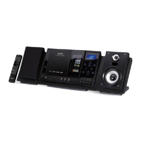
Sony HCD-GNX80 User manual

HCD-GNX80
E Model
Australian Model
SERVICE MANUAL
MiNi Hi-Fi COMPONENT SYSTEM
Sony Corporation
Audio Group
Published by Sony Engineering Corporation
9-879-460-01
2005B02-1
© 2005.02
SPECIFICATIONS
Ver.1.0 2005. 02
– Continued on next page –
•HCD-GNX80 is the Amplifier,
CD player, tape deck and tuner
section in MHC-GNX80.
Model Name Using Similar Mechanism HCD-GN880
CD CD Mechanism Type CDM74-F1BD81
Section Base Unit Name BU-F1BD81A
Optical Pick-up Name KSM-215DCP/C2NP
TAPE Model Name Using Similar Mechanism NEW
Section Tape Transport Mechanism Type CMAT5Z2
The following are measured at
AC 120, 220, 240 V, 50/60 Hz
DIN power output (rated) 180 + 180 watts
(6 ohms at 1 kHz, DIN)
Continuous RMS power output (reference)
225 + 225 watts
(6 ohms at 1 kHz, 10% THD)
Inputs
VIDEO/MD (AUDIO) IN (phono jacks):
voltage 250/450 mV,
impedance 47 kiloohms
TV (AUDIO) IN (phono jack): voltage 250 mV,
impedance 47 kiloohms
MIC (phone jack): sensitivity 1 mV,
impedance 10 kiloohms
Outputs
PHONES (stereo mini jack): accepts headphones of
8 ohms or more
FRONT SPEAKER: Use only the supplied speaker
• SS-GNX100
SURROUND SPEAKER: Use only the supplied speaker
• SS-RSX80
SUBWOOFER OUT: Use only the supplied subwoofer
• SS-WG80
Disc player section
System Compact disc and digital audio system
Laser Semiconductor laser (λ=780 nm)
Emission duration: continuous
Laser Output Max. 44.6 µW*
*This output is the value measured at a
distance of 200 mm from the objective
lens surface on the Optical Pick-up Block
with 7 mm aperture.
Frequency response 2 Hz – 20 kHz (±0.5 dB)
Wave length 780 – 790 nm
Signal-to-noise ratio More than 90 dB
Dynamic range More than 90 dB
OPTICAL CD DIGITAL OUT
(Square optical connector jack, rear panel)
Wave length 660 nm
Output Level –18 dBm

2
HCD-GNX80
Notes on chip component replacement
•Never reuse a disconnected chip component.
•Notice that the minus side of a tantalum capacitor may be
damaged by heat.
Flexible Circuit Board Repairing
•Keep the temperature of soldering iron around 270˚C
during repairing.
•Do not touch the soldering iron on the same conductor of the
circuit board (within 3 times).
•Be careful not to apply force on the conductor when soldering
or unsoldering.
CAUTION
Use of controls or adjustments or performance of procedures
other than those specified herein may result in hazardous
radiation exposure.
This appliance is classified as
a CLASS 1 LASER product.
This label is located on the rear
exterior.
SAFETY-RELATED COMPONENT WARNING!!
COMPONENTS IDENTIFIED BY MARK 0OR DOTTED LINE WITH
MARK 0ON THE SCHEMATIC DIAGRAMS AND IN THE PARTS
LIST ARE CRITICAL TO SAFE OPERATION. REPLACE THESE
COMPONENTS WITH SONY PARTS WHOSE PART NUMBERS
APPEAR AS SHOWN IN THIS MANUAL OR IN SUPPLEMENTS
PUBLISHED BY SONY.
Tape deck section
Recording system 4-track 2-channel stereo
Frequency response 50 – 13,000 Hz (±3 dB),
using Sony TYPE I tape
Tuner section
FM stereo, FM/AM superheterodyne tuner
FM tuner section
Tuning range 87.5 – 108.0 MHz
Antenna FM lead antenna
Antenna terminals 75 ohm unbalanced
Intermediate frequency 10.7 MHz
AM tuner section
Tuning range
North and Latin American models:
530 – 1,710 kHz
(with the interval set at 10 kHz)
531 – 1,710 kHz
(with the interval set at 9 kHz)
Other models: 531 – 1,602 kHz
(with the interval set at 9 kHz)
530 – 1,710 kHz
(with the interval set at 10 kHz)
Antenna AM loop antenna
Antenna terminals External antenna terminal
Intermediate frequency 450 kHz
General
Power requirements
Australian model: 230 – 240 V AC, 50/60 Hz
Other models: 120 V, 220 V or 230 – 240 V AC,
50/60 Hz
Adjustable with voltage selector
Power consumption 350 W
Dimensions (w/h/d) (Approx.) 280 x 360 x 398.5 mm
Mass (Approx.)
Supplied accessories: Remote Commander (1)
Batteries (2)
AM loop antenna (1)
FM lead antenna (1)
Front speaker pads (8)
Surround speaker pads (8)
Subwoofer pads (4)
Design and specifications are subject to change without notice.
Unleaded solder
Boards requiring use of unleaded solder are printed with the lead
free mark (LF) indicating the solder contains no lead.
(Caution: Some printed circuit boards may not come printed with
the lead free mark due to their particular size.)
: LEAD FREE MARK
Unleaded solder has the following characteristics.
•Unleaded solder melts at a temperature about 40°C higher than
ordinary solder.
Ordinary soldering irons can be used but the iron tip has to be
applied to the solder joint for a slightly longer time.
Soldering irons using a temperature regulator should be set to
about 350°C.
Caution: The printed pattern (copper foil) may peel away if
the heated tip is applied for too long, so be careful!
•Strong viscosity
Unleaded solder is more viscous (sticky, less prone to flow)
than ordinary solder so use caution not to let solder bridges
occur such as on IC pins, etc.
•Usable with ordinary solder
It is best to use only unleaded solder but unleaded solder may
also be added to ordinary solder.

3
HCD-GNX80
TABLE OF CONTENTS
1. SERVICING NOTES ................................................ 4
2. GENERAL
Location of Controls ........................................................ 5
3. DISASSEMBLY
3-1. Disassembly Flow ........................................................... 7
3-2. Side Panel, Top Case ....................................................... 8
3-3. Loading Panel Assy ......................................................... 8
3-4. Front Panel Assy .............................................................. 9
3-5. Tuner Pack ....................................................................... 9
3-6. Tape Mechanism Deck, Mic Board ................................. 10
3-7. Panel Board, CD-SW Board ............................................ 10
3-8. CD Mechanism Deck ...................................................... 11
3-9. Back Panel ....................................................................... 11
3-10. Primary Board ................................................................. 12
3-11. Power AMP PC Board Assy, Main Board ....................... 12
3-12. Surround Board, PA Board .............................................. 13
3-13. Power Transformer (T1200) ............................................ 13
3-14. Driver Board, SW Board ................................................. 14
3-15. CD Board ......................................................................... 14
3-16. Sensor Board ................................................................... 15
3-17. Motor (TB) Board ........................................................... 15
3-18. Motor (LD) Board ........................................................... 16
4. TEST MODE .............................................................. 17
5. MECHANICAL ADJUSTMENTS ....................... 21
6. ELECTRICAL ADJUSTMENTS
Deck section .................................................................... 21
CD Section ...................................................................... 22
7. DIAGRAMS
7-1. Circuit Board Location .................................................... 26
7-2. Block Diagram – CD Section – ...................................... 27
7-3. Block Diagram – Tape Section – .................................... 28
7-4. Block Diagram – Main Section – ................................... 29
7-5. Block Diagram – AMP Section – ................................... 30
7-6. Block Diagram – Display Section – ............................... 31
7-7. Printed Wiring Board – CD Board – .............................. 32
7-8. Schematic Diagram – CD Board – ................................. 33
7-9. Printed Wiring Board – CD Mechanism Board – ........... 34
7-10. Schematic Diagram – CD Mechanism Board – ............. 35
7-11. Printed Wiring Boards – Main Board – .......................... 36
7-12. Schematic Diagram – Main Board (1/3) – ..................... 37
7-13. Schematic Diagram – Main Board (2/3) – ..................... 38
7-14. Schematic Diagram – Main Board (3/3) – ..................... 39
7-15. Printed Wiring Boards – Panel Board – ......................... 40
7-16. Schematic Diagram – Panel Board – ............................... 41
7-17. Printed Wiring Board – CD-SW, Jog, Mic Boards – ...... 42
7-18. Schematic Diagram – CD-SW, Jog, Mic Board – .......... 43
7-19. Printed Wiring Board – PA Board – ............................... 44
7-20. Schematic Diagram – PA Board – .................................. 45
7-21. Printed Wiring Board – Surround Board – ..................... 46
7-22. Schematic Diagram –Surround Board – ......................... 47
7-23. Printed Wiring Board – Trans, Primary Boards – .......... 48
7-24. Schematic Diagram – Trans, Primary Boards – ............. 49
7-25. IC Pin Function Description ............................................ 52
8. EXPLODED VIEWS
8-1. Case (Top), Rear Panel Section ....................................... 58
8-2. Front Panel Section ......................................................... 59
8-3. Chassis Section ................................................................ 60
8-4. CD Mechanism Deck Section-1
(CDM74-F1BD81) .......................................................... 61
8-5. CD Mechanism Deck Section-2
(CDM74-F1BD81) .......................................................... 62
9. ELECTRICAL PARTS LIST ................................ 63

4
HCD-GNX80
SECTION 1
SERVICING NOTES
NOTES ON HANDLING THE OPTICAL PICK-UP BLOCK
OR BASE UNIT
The laser diode in the optical pick-up block may suffer electrostatic
break-down because of the potential difference generated by the
charged electrostatic load, etc. on clothing and the human body.
During repair, pay attention to electrostatic break-down and also
use the procedure in the printed matter which is included in the
repair parts.
The flexible board is easily damaged and should be handled with
care.
NOTES ON LASER DIODE EMISSION CHECK
The laser beam on this model is concentrated so as to be focused on
the disc reflective surface by the objective lens in the optical pick-
up block. Therefore, when checking the laser diode emission, observe
from more than 30 cm away from the objective lens.
LASER DIODE AND FOCUS SEARCH OPERATION CHECK
Carry out the “S curve check” in “CD section adjustment” and check
that the S curve waveform is output several times.
•MODEL IDENTIFICATION
– Back Panel –
MODEL PART No.
E2, E3 models 2-547-459-0[]
E51model 2-588-970-0[]
AUS model 2-588-969-0[]
•Abbreviation
E2 : 120 V AC Area in E model
E3 : 240 V AC Area in E model
E51 : Chilean and Peruvian model
AUS : Australian model
PA R T No.

5
HCD-GNX80
SECTION 2
GENERAL This section is extracted
from instruction manual.
LOCATING THE CONTROLS
Main unit
ALBUM +/– ql
AMP MENU ed
AUTO/MANUAL
3)
2
CD el
CD SYNC qd
Deck A ea
Deck B ws
DIRECTION qk
DISC 1 ~ 3 7
Disc tray 9
DISPLAY rd
Display rf
ECHO LEVEL wf
ENTER wa
EQ BAND qa
EX-CHANGE/DISC SKIP 6
GROOVE eh
ILLUMINATION rs
IR Receptor r;
MASTER VOLUME 8
MIC 1 (jack) wj
MIC 2 (jack) wh
MIC LEVEL wg
MP3 BOOSTER q;
MPX
4)
qk
OPERATION DIAL wl
PHONES (jack) wk
Power illuminator wd
REC PAUSE/START qh
SOUND FLASH e;
SPEAKERS
3)
1
SURROUND
1)
rg
SURR SPEAKER MODE
2)
rg
TA PE A/B ej
Ta pe lid ws ea
TUNER/BAND ek
TUNING +/– qj
TV eg
VIDEO/MD ef
X-ROUND buttons
3)
3
WA VE/FADER/BALANCE/
RANDOM/TWISTER
X-ROUND JOG
3)
4
X-ROUND OFF
3)
1
?/1 (power) ra
ZOPEN/CLOSE 5
nN(play) qs
. > (go backward/forward) qj
m M (rewind/fast forward) ql
X(pause) qf
x(stop) qg
ZA (Eject A) es
BZ(Eject B) w;
1)
For MHC-GNX100/GNX66/
GNX60
2)
For MHC-GNX88/GNX80/
GNX77/GNX70/GX9900
3)
MHC-GNX100 only
4)
For MHC-GNX88/GNX77/
GNX66
List of button locations and reference pages
ALPHABETICAL ORDER
A – D
E – L
M – R
S – Z
SYMBOLS
Top Panel
Front Panel
4
657
12 3
wk wgwhwj wf
qj
qk
ql
w; wz
ws wd
rg
rd
ra
el
ej
eg
wl
e;
ea
es ed
ef
eh
ek
r;
rs
rf 8
0
qa
qs qd
qf
qg
qh
9

6
HCD-GNX80
This section is extracted
from instruction manual.
Remote control
ALBUM + qf
ALBUM – qh
CD wf
CLEAR qk
CLOCK/TIMER SELECT 2
CLOCK/TIMER SET 4
DISC SKIP qd
DISPLAY wh
ENTER qs
EQ qj
FM MODE 6
FUNCTION 8
PLAY MODE 5
REPEAT 6
SLEEP 1
TA PE wd
TUNER/BAND 7
TUNER MEMORY wg
TUNING MODE 5
VOLUME +/– qg
The + button has a tactile dot.*
?/1 (power) 3
x(stop) qa
X(pause) ql
N (play) w;
–.(go backward) ws
>+ (go forward) wa
m(rewind) q;
M(fast forward) 9
*Usethetactile dot as a reference
when operating the system.
ALPHABETICAL ORDER
A – E
F – Z
SYMBOLS
7
5
q;
qg
qh
qj
qk
w;
ws
wd
wg
wh
qf
qd
qs
qa
9
8
6
4
312
ql
wa
wf

7
HCD-GNX80
SECTION 3
DISASSEMBLY
• This set can be disassembled in the order shown below.
3-1. DISASSEMBLY FLOW
3-2.SIDE PANEL, TOP CASE
(Page 8)
3-3.LOADING PANEL ASSY
(Page 8)
3-4.FRONT PANEL ASSY
(Page 9)
3-5.TUNER PACK
(Page 9)
3-13.POWER TRANSFORMER
(T1200)
(Page 13)
3-11.POWER AMP PC BOARD ASSY,
MAIN BOARD
(Page 12)
3-8.CD MECHANISM DECK
(Page 11)
3-7.PANEL BOARD,
CD-SW BOARD
(Page 10)
3-6.TAPE MECHANISM DECK,
MIC BOARD
(Page 10)
3-14.DRIVER BOARD,
SW BOARD
(Page 14)
3-10.PRIMARY BOARD
(Page 12) 3-17.MOTOR (TB) BOARD
(Page 15)
3-18.MOTOR (LD) BOARD
(Page 16)
3-16.SENSOR BOARD
(Page 15)
3-12.SURROUND BOARD,
PA BOARD
(Page 13)
3-9.BACK PANEL
(Page 11)
3-15.CD BOARD
(Page 14)
SET

8
HCD-GNX80
Note: Follow the disassembly procedure in the numerical order given.
3-2. SIDE PANEL, TOP CASE
3-3. LOADING PANEL ASSY
1
screw (case 3 TP2)
(3X8)
2
two screws
(case 3 TP2)
(3X12)
3
two screws
(+BVTP 3X10)
4
5
PANEL (SIDE-L)
6
screw
(case 3 TP2)
(3X8)
7
two screws
(case 3 TP2)
(3X12)
8
two screws
(+BVTP 3X10)
9
0
PANEL (SIDE-R)
qa
two screws
(+BVTP 3X10)
qs
qd
CASE (TOP)
CD mechanismdeck (CDM74-F1BD81)
1
Turn the pulley to the arrow direction.
Front side
Pulley
2
Pull out disc tray
3
4
loading panel assy

9
HCD-GNX80
3-4. FRONT PANEL ASSY
3-5. TUNER PACK
1
two screws
(+BVTP 3X10)
2
two screws
(+BVTP 3X10)
3
screw
(+BVTP 3X10)
5
screw
(+BVTP 3X6)
4
screw
(+BVTP 3X10)
6
front panel assy
7
connector
(CN100)
8
CNP508
9
CNP509
q;
connector
(CN503)
lug
qa
connector
(CN1102)
qs
connector
(tape mechanism deck)
1
two screws
(+BVTP 3X6)
2
CNP1
3
tuner pack

10
HCD-GNX80
3-6. TAPE MECHANISM DECK, MIC BOARD
3-7. PANEL BOARD, CD-SW BOARD
1
two screws
(+BVTP2.6 (3CR)
)
3
cover (TCM)
2
two screws
(+BVTP2.6 (3CR))
4
screw
(+BVTP2.6 (3CR))
5
tape mechanism deck
6
two screws
(+BVTP2.6 (3CR))
7
bracket (MIC)
9
MIC board
8
knob (MIC)
1
knob vol
2
knob (AMS)
3
three screws
(+BVTP2.6 (3CR))
4
two screws
(+BVTP2.6 (3CR))
5
two screws
(+BVTP2.6 (3CR))
6
two screws
(+BVTP2.6 (3CR))
7
three screws
(+BVTP2.6 (3CR))
8
connector
(CNS902)
0
PANEL board
qa
CD-SW board
9
claw
Other manuals for HCD-GNX80
1
Table of contents
Other Sony Stereo System manuals

Sony
Sony HCD-XB88AVK User manual

Sony
Sony CMT-L7HD - Micro Hi Fi Component System User manual

Sony
Sony PHC-ZW770L User manual

Sony
Sony LBT-XB5 User manual

Sony
Sony MHC-GN900 User manual

Sony
Sony BMZ-K2 User manual

Sony
Sony HCD-FX300i US User manual

Sony
Sony ICF-DS15iPN User manual

Sony
Sony MHC-RX70 User manual

Sony
Sony MEX-M100BT User manual

Sony
Sony CDP-X3000 User manual

Sony
Sony FH-411R User manual

Sony
Sony MHC-V44D User manual

Sony
Sony Giga Juke NAS-SC500PK User manual

Sony
Sony MDS-S500 User manual

Sony
Sony CMT-M80V User manual

Sony
Sony HCD-CP300 User manual

Sony
Sony LBT-D107R User manual

Sony
Sony HCD-GZR888D User manual

Sony
Sony GTK-XB60 User manual