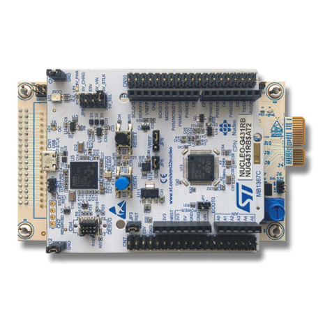
Mesa 7I46 User manual

7I46 MANUAL
6 channel SPI breakout
V1.0

This page intentionally almost blank

iii
Table of Contents
GENERAL . . . . . . . . . . . . . . . . . . . . . . . . . . . . . . . . . . . . . . . . . . . . . . . . . . . . . . . . . . 1
DESCRIPTION . . . . . . . . . . . . . . . . . . . . . . . . . . . . . . . . . . . . . . . . . . . . . . . . . 1
HARDWARE CONFIGURATION . . . . . . . . . . . . . . . . . . . . . . . . . . . . . . . . . . . . . . . . 2
TERMINATION ENABLE . . . . . . . . . . . . . . . . . . . . . . . . . . . . . . . . . . . . . . . . . 2
CONNECTORS . . . . . . . . . . . . . . . . . . . . . . . . . . . . . . . . . . . . . . . . . . . . . . . . . . . . . . 3
CONNECTOR LOCATIONS AND DEFAULT JUMPERS . . . . . . . . . . . . . . . . . 3
CONTROLLER CONNECTOR . . . . . . . . . . . . . . . . . . . . . . . . . . . . . . . . . . . . . 4
AUX 5V POWER . . . . . . . . . . . . . . . . . . . . . . . . . . . . . . . . . . . . . . . . . . . . . . . 4
SPI CONNECTORS . . . . . . . . . . . . . . . . . . . . . . . . . . . . . . . . . . . . . . . . . . . . . 5
OPERATION
5VPOWER ................................................... 6
SPECIFICATIONS . . . . . . . . . . . . . . . . . . . . . . . . . . . . . . . . . . . . . . . . . . . . . . . . . . . 7

7I47 1
GENERAL
DESCRIPTION
The 7I46 is a simple passive breakout board designed to connect up to 6 SPI
devices to a single 50 pin Anything I/O connector. 10 pin headers are used for the SPI
signals. The pinout matches Mesas SPI device pinouts andalso supplies 5V power to the
SPI device. A high side power switch allows AUX 5V power suppled to the the 7I46 to be
routed to the SPI devices, the SPI power will be removed when the Anything I/Os cable
power is off, avoiding possible back-powering of the FPGA card from external AUX 5V
supply.
The controller connection is a 50 pin header that matches the pinout of Mesa’s
Anything I/O cards. All RS-422 interface connections use pluggable Phoenix compatible
3.5 mm screw terminals.

7I47 2
HARDWARE CONFIGURATION
GENERAL
Hardwaresetupjumperpositionsassumethatthe7I46cardisorientedinanupright
position, that is, with the 50 pin controller connector is on the left hand side.
DEFAULT CONFIGURATION
JUMPER FUNCTION DEFAULT SETTING
W1 CABLE/AUX 5V POWER UP = CABLE POWER
CABLE POWER ENABLE
The7I46can supplyI/O powertoP2throughP7 viaTB1or viathe50 conductorflat
cable. If W1 is in the"UP" position, flat cable power is used. If W1 is on the "DOWN"
position, TB1 power is used.

7I47 3
CONNECTORS
CONNECTOR LOCATIONS AND DEFAULT JUMPER POSITIONS

7I47 4
CONNECTORS
CONTROLLER CONNECTOR
50pinheaderconnectorJ1connectstotheanythingI/Ocard/motioncontroller.This
can be a male 50 pin header on the top of the 7I46 card or a female 50 conductor header
on the bottom side of the 7I46 depending on 7I46 model.
PIN FUNCTION DIRECTION PIN FUNCTION DIRECTION
1 FRAME0 TO 7I46 25 FRAME3 TO 7I46
3 DOUT0 TO 7I46 27 DOUT3 TO 7I46
5 CLK0 TO 7I46 29 CLK3 TO 7I46
7 DIN0 FROM 7I46 31 DIN3 FROM 7I46
9 FRAME1 TO 7I46 33 FRAME4 TO 7I46
11 DOUT1 TO 7I46 35 DOUT4 TO 7I46
13 CLK1 TO 7I46 37 CLK4 TO 7I46
15 DIN1 FROM 7I46 39 DIN4 FROM 7I46
17 FRAME2 TO 7I46 41 FRAME5 TO 7I46
19 DOUT2 TO 7I46 43 DOUT5 TO 7I46
21 CLK2 TO 7I46 45 CLK5 TO 7I46
23 DIN2 FROM 7I46 47 DIN5 FROM 7I46
49 +5V PWR TO 7I46
Note: all even pins are grounded. Signal names shown are for SPI interface on
FPGA card. Since the 7I46 is a passive device the 7I46 breakout can be used
for other signal types.
AUX 5V POWER
2 pin pluggable terminal TB1 can beused to supply5V power to theSPIconnectors
on the7I46. This is suggested for most applications as the SPI devices will typically will
draw more current than can be supplied via the FPGA flat cable. TB1 has the following
pinout:
PIN FUNCTION
1 5V
2 GND

7I47 5
CONNECTORS
SPI CONNECTOR PINOUT
TheSPI connectorsare10pin.1"pitchmaleheaders.Suggestedmatingconnector
is AMP PN 1658622-1. This is an IDC receptacle for 10 conductor .050 flat cable. SPI
signal integrity depends on wiring order, soif flat cableis not used, the SPI cable must use
twisted pairs, with each SPI signal twisted with its adjacent ground signal.
All SPI connectors (P2 through P7) have the same pinout:
PIN FUNCTION DIR
1 +5V FROM 7I46
2 GND TO 7I46
3 FRAME(N) FROM 7I46
4 GND FROM 7I46
5 DOUT(N) FROM7I46
6 GND FROM 7I46
7 CLK(N) FROM 7I46
8 GND FROM 7I46
9 DIN(N) TO 7I46
10 +5V FROM 7I46
"N" is the SPI channel, the SPI connectors and channels are as follows:
SPI CONNECTOR SPI CHANNEL
P2 0
P3 1
P4 2
P5 3
P6 4
P7 5

7I47 6
OPERATION
5V POWER
The 7I46 being passive requires no 5V power for operation, the SPI channels
however may draw up to 500 mA of current per channel. This power will normally be
supplied via TB1. For testing and with low power SPI devices, the SPI connectors can get
their power from the controller cable
If W1 is on the "UP" position, the controller cable will supply the SPI connector
power and T1 can remain unconnected. This mode can be used for testing but it is
suggested that W1 be placed inthe "DOWN" position and SPI power be supplied via TB1
for most applications.
The power from connector TB1 Passes through a 3.75A PTC device before being
routed to the I/O terminals. This limits the total I/O power supplied by the 7I46 to ~3 A in
0 to 70C ambients.
Notethatthe5VpowersuppliedtotheSPIconnectorsviaTB1isswitchedbyahigh
side switch that disconnect the SPI devices power when cable power is lost. This is done
to prevent back-powering the FPGA card from SPI outputs when the FPGA card is
powered down.

7I47 7
SPECIFICATIONS
MIN MAX UNITS
5V POWER SUPPLY 4.75 5.25 VDC
MAXIMUM POWER TO I/O CONNECTORS --- 500 mA
Per SPI connector
OPERATING TEMP. 0 +70 oC
OPERATING TEMP. (-I version) -40 +85 oC
OPERATION HUMIDITY 0 95% NON-COND
Table of contents
Other Mesa Motherboard manuals