AMD XILINX VPK180 User manual

VPK180 Evaluaon Board
User Guide
UG1582 (v1.0) February 21, 2023
Xilinx is creating an environment where employees, customers, and
partners feel welcome and included. To that end, we’re removing non-
inclusive language from our products and related collateral. We’ve
launched an internal initiative to remove language that could exclude
people or reinforce historical biases, including terms embedded in our
software and IPs. You may still find examples of non-inclusive language
in our older products as we work to make these changes and align
with evolving industry standards. Follow this link for more
information.

Table of Contents
Chapter 1: Introduction.............................................................................................. 4
Overview.......................................................................................................................................4
Navigating Content by Design Process.................................................................................... 5
Additional Resources.................................................................................................................. 5
Block Diagram..............................................................................................................................6
Board Features............................................................................................................................ 7
Board Specifications................................................................................................................. 10
Chapter 2: Board Setup and Configuration....................................................12
Standard ESD Measures........................................................................................................... 12
Board Component Location.....................................................................................................12
Default Jumper and Switch Settings....................................................................................... 18
Versal ACAP Configuration.......................................................................................................21
Chapter 3: Board Component Descriptions................................................... 23
Overview.....................................................................................................................................23
Component Descriptions......................................................................................................... 23
Appendix A: VITA 57.4 FMCP Connector Pinouts......................................... 71
Overview.....................................................................................................................................71
Appendix B: Xilinx Design Constraints............................................................. 72
Overview.....................................................................................................................................72
Appendix C: Regulatory and Compliance Information........................... 73
CE Information...........................................................................................................................73
Compliance Markings............................................................................................................... 74
Appendix D: Additional Resources and Legal Notices.............................75
Xilinx Resources.........................................................................................................................75
Documentation Navigator and Design Hubs.........................................................................75
References..................................................................................................................................76
UG1582 (v1.0) February 21, 2023 www.xilinx.com
VPK180 Board User Guide 2
Send Feedback

Revision History.........................................................................................................................77
Please Read: Important Legal Notices................................................................................... 77
UG1582 (v1.0) February 21, 2023 www.xilinx.com
VPK180 Board User Guide 3
Send Feedback

Chapter 1
Introduction
Overview
The VPK180 evaluaon board features the Xilinx® Versal® ACAP XCVP1802 device. The
VPK180 board enables the demonstraon, evaluaon, and development of the applicaons listed
here, as well as other customer applicaons. Many features found on the VPK180 board are
subsets of exisng Versal ACAP boards (e.g., the VCK190 and VMK180 boards).
• Fiber opc
•Communicaons
• Data center compute acceleraon
• Aerospace and defense
• Test and measurement
The VPK180 evaluaon board is equipped with many of the common board-level features
needed for design development, including:
• OSFP opcal transceiver support
• QSFP-DD opcal transceiver support
• SFP-DD opcal transceiver support
• LPDDR4 component memory
• USB
• Ethernet networking interface
• One FMC+ expansion port
Models of Boards
The following table lists the models for the VPK180 evaluaon board. See the VPK180
Evaluaon Board product page for details
Chapter 1: Introduction
UG1582 (v1.0) February 21, 2023 www.xilinx.com
VPK180 Board User Guide 4
Send Feedback
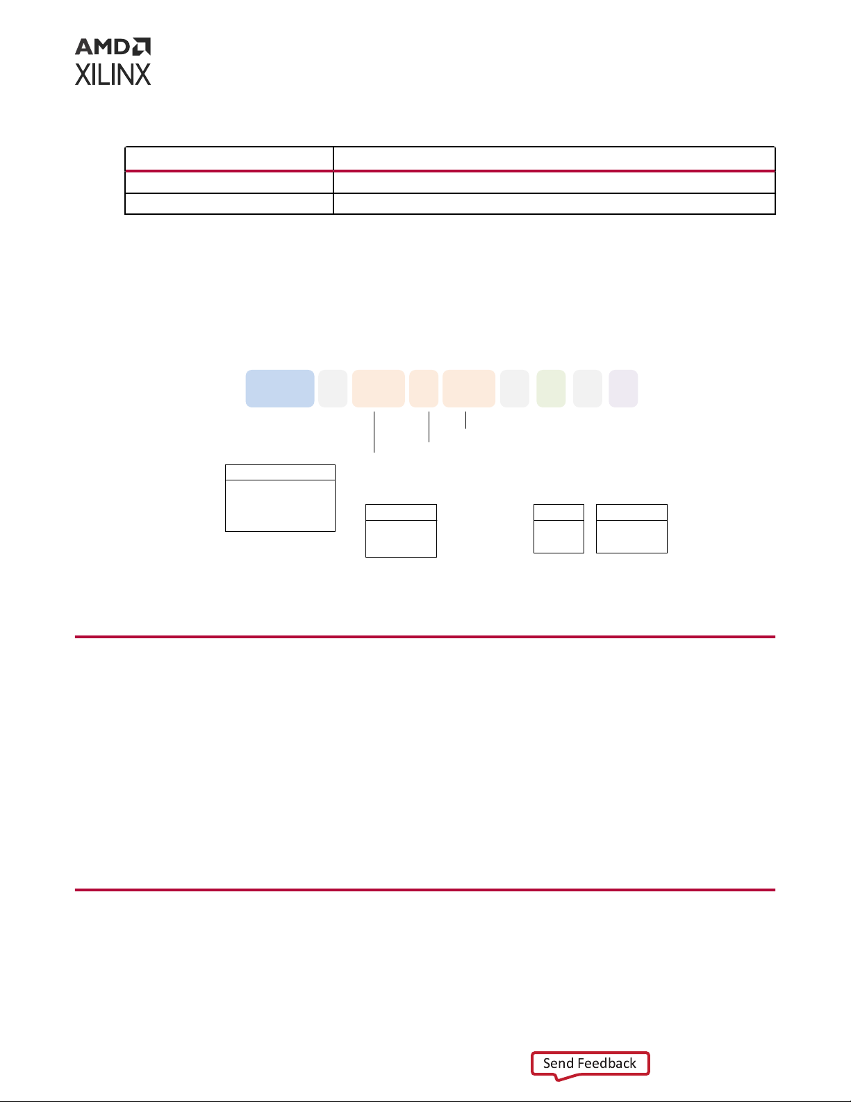
Table 1: Models of VPK180 Evaluation Boards
Kit Description
EK-VPK180-G Xilinx Versal ACAP VPK180 evaluation kit
EK-VPK180-G-J Xilinx Versal ACAP VPK180 evaluation kit, Japan specific
Versal ACAP Kit Numbering
The Versal ACAP kit numbering is illustrated in the following gure.
Figure 1: Kit Numbering
EK - VP
Kit
Type
Options
EK –Evaluation Kit
CK –Characterization Kit
K 180 - G - J
ROHS
Indicator
Regional
Identifier
Silicon indicator
K = kit
Ensures there is no
confusion with silicon P/Ns
Family and series
(e.g., Versal ACAP
and Core)
Examples
VPK120
VCK190
Options
G –ROHS
Compliant
Options
J –Japan
OEM –OEM kit
Product Number
X26520-111822
Navigating Content by Design Process
Xilinx® documentaon is organized around a set of standard design processes to help you nd
relevant content for your current development task. All Versal® ACAP design process Design
Hubs and the Design Flow Assistant materials can be found on the Xilinx.com website. This
document covers the following design processes:
•Board System Design: Designing a PCB through schemacs and board layout. Also involves
power, thermal, and signal integrity consideraons. For more informaon, see Versal ACAP
Design Process Documentaon Board System Design.
Additional Resources
See Appendix D: Addional Resources and Legal Noces for references to documents, les, and
resources relevant to the VPK180 evaluaon board.
Chapter 1: Introduction
UG1582 (v1.0) February 21, 2023 www.xilinx.com
VPK180 Board User Guide 5
Send Feedback

Block Diagram
A block diagram of the VPK180 evaluaon board is shown in the following gure.
Figure 2: Evaluation Board Block Diagram
GTYP
GTYP
GTM
GTM
GTM
GTM
GTM
PS/
PMC
2x LPDDR4
(1x32)
2x QSPI
GPIO 3.3V
SFP/QSFP/
OSFP Ctrl
FMC+
(XPIO)
2x LPDDR4
(1x32)
USB 2.0 ULPI
SD 3.0
UART/I2C
GEM 2x LPDDR4
(1x32) EMIO
Mictor
1588 CLK SMAs
SysC
GPIO
Lvl
Shftrs
GTM
GTM
GTM
GTM
GTM
GTM
GTM
GTM
GTM
GTM
QSFPDD_3
56G capable
SFPDD_2
56G/112G capable
SFPDD_1
56G/112G capable
QSFPDD_1
112G capable
QSFPDD_2
56G capable
GTM
GTM
GTM
GTM
GTM
GTM
GTM
GTM
GTM
GTM
QSFPDD_4
56G capable
SFPDD_4
56G/112G capable
SFPDD_3
56G/112G capable
OSFP
GTM
GTM
GTM
GTM
GTM
GTM
GTM
GTM
GTM
GTM
QSFPDD_5
112G capable
QSFPDD_6
112G capable
Power Enables
SLR Crossing
SLR Crossing
SLR Crossing
124
123
122
121
118
117
116
115
112
111
110
109
206
205
204
203
202
201
200
212
211
210
209
208
207
218
217
216
215
214
213
224
223
222
221
220
219
HSDP
USB Type-C
HSDP
SYSCTLR GTH
1588 SMA
Versal XCVP1802
LSVC4072
XPIO
GTYP
GTYP
GTYP
GTYP
GTYP
106
105
104
103
102
Lvl
Shftrs
X26519-110222
Chapter 1: Introduction
UG1582 (v1.0) February 21, 2023 www.xilinx.com
VPK180 Board User Guide 6
Send Feedback
Board Features
The VPK180 evaluaon board features are listed here. Detailed informaon for each feature is
provided in Chapter 3: Board Component Descripons.
• XCVP1802, LSVC4072 package
• Form factor: see Board Specicaons
• Onboard conguraon from:
○USB-to-JTAG bridge
○JTAG pod 2 mm 2x7 at cable connector
○microSD card (PS MIO I/F)
○Quad SPI (QSPI)/eMMC (system controller I/F)
○Dual QSPI
• Clocks
○ACAP bank 702/5/8 Si570 LPDDR4_CLK1/2/3 (DIMM) 200 MHz
○ACAP bank 503 Si570 REF_CLK 33.3333 MHz
○ACAP bank 503 RTC Xtal 32.768 kHz
○IEEE-1588 eCPRI 8A34001 clocks (various)
○ACAP bank GTY102/4 (REFCLK0) HSDP dedicated clocks
○ACAP bank GTY200/1 (REFCLK0) FMC provided
○ACAP banks GTM109, GTM110, GTM111, GTM112, GTM115, GTM116, GTM117,
GTM118 RC21008A 156.25 MHz
○ACAP banks GTM208, GTM209, GTM210, GTM211, GTM214, GTM215, GTM216,
GTM217 RC21008A 156.25 MHz
• Three LPDDR4 interfaces (2x32-bit 4 GB components each)
○XPIO triplet 1 (banks 700, 701, 702)
○XPIO triplet 2 (banks 703, 704, 705)
○XPIO triplet 3 (banks 706, 707, 708)
• PL FMCP HSPC (FMC+) connecvity
○FMCP1 HSPC full LA[00:33] bus
Chapter 1: Introduction
UG1582 (v1.0) February 21, 2023 www.xilinx.com
VPK180 Board User Guide 7
Send Feedback

• PL GPIO connecons
○PL UART1 to FTDI
○PL GPIO DIP switch (4-posion)
○PL GPIO LEDs (four)
○PL GPIO pushbuons (two)
○PL trace connector (J332)
○PL SYSCTLR_GPIO[0:15]
○PL 8A34001_GPIO[0:7, 10:15]
• 28 PL GTYP transceivers (7 quads)
○Not used (18, bank GTYP102, GTYP103, GTYP104, GTYP105, GTYP106)
○System controller HSDP (1, banks GTYP104)
○USB-C HSDP (1, banks GTYP102)
○FMCP1 HSPC DP (8, banks GTYP200, GTYP201)
• 140 PL GTM transceivers (35 quads)
○Not used (74, bank GTM109, GTM110, GTM115, GTM116, GTM121, GTM122, GTM123,
GTM124, GTM202, GTM203, GTM204, GTM205, GTM206, GTM207, GTM212,
GTM213, GTM214, GTM215, GTM216, GTM217, GTM218, GTM219, GTM220,
GTM221, GTM222, GTM223, GTM224)
○QSFPDD1 (8, banks GTM208, GTM209, GTM210, GTM211)
○QSFPDD2 (8, banks GTM208, GTM209, GTM210, GTM211)
Note: QSFPDD1 and QSFPDD2 are interleaved.
○QSFPDD3 (8, banks GTM111, GTM112)
○QSFPDD4 (8, banks GTM117, GTM118)
○QSFPDD5 (8, banks GTM121, GTM122, GTM123, GTM124)
○QSFPDD6 (8, banks GTM221, GTM222, GTM223, GTM224)
○OSFP (8, banks GTM214, GTM215, GTM216, GTM217)
○SFPDD1 (2, bank GTM109)
○SFPDD2 (2, bank GTM110)
○SFPDD3 (2, bank GTM115)
○SFPDD4 (2, bank GTM116)
Chapter 1: Introduction
UG1582 (v1.0) February 21, 2023 www.xilinx.com
VPK180 Board User Guide 8
Send Feedback

○User SMA connectors (1, bank GTM219)
○8A34001 CLK (1, bank GTM219)
• PS PMC MIO connecvity
○PS MIO[0:12]: boot conguraon QSPI
- DC QSPI support
○PS MIO[13:25]: USB2.0
○PS MIO[26:36, 51]: SD1 I/F
○PS MIO[37]: ZU4_TRIGGER
○PS MIO[38]: Not connected
○PS MIO[39:41]: SYSMON_I2C
○PS MIO[42:43]: UART0 to FTDI
○PS MIO[44:47]: I2C1, I2C0
○PS MIO[48], PS LPD MIO[0:11, 24:25]: GEM0 RGMII Ethernet RJ-45
○PS MIO[49] and LPD MIO[13,15:16,20]: power enable
○PS MIO[50] and LPD MIO[18:19]: Not connected
○PS LPD MIO [21:22]: oponal fan interface
○LPD MIO[23]: VADJ_FMC power rail
• Security: PSBATT buon baery backup
• SYSMON header
•Operaonal switches (power on/o, PROG_B, boot mode DIP switch)
•Operaonal status LEDs (INIT, DONE, PS STATUS, PGOOD)
○See Power and Status LEDs
• Power management
• System controller (XCZU4EG)
The VPK180 evaluaon board provides a rapid prototyping plaorm using the
XCVP1802-2MSELSVC4072 device. See the Versal Architecture and Product Data Sheet: Overview
(DS950) for a feature set overview, descripon, and ordering informaon.
Chapter 1: Introduction
UG1582 (v1.0) February 21, 2023 www.xilinx.com
VPK180 Board User Guide 9
Send Feedback

Board Specifications
Dimensions
Height: 12.360 inches (31.394 cm)
Length: 11.504 inches (29.22016 cm)
Thickness: 131.5 mil ±10% (3.3401 ±10%)
Note: A 3D model of this board is not available.
See the VPK180 Evaluaon Board website for the XDC lisng and board schemacs.
Environmental
Note: The operang temperature range is not fully tested across the specied temperature range. It is for
general guidelines only. Customers should use the VPK180 evaluaon board for evaluaon purposes only
in a normal lab environment and should not operate beyond room temperature.
•Temperature:
Operang: 0°C to +45°C
Storage: –25°C to +60°C
•Humidity: 5% to 95% non-condensing
Operating Voltage
+12 VDC
Mechanical
The VPK180 evaluaon board includes a mechanical sener to help ensure success with the
board under normal lab condions and use. While it is recommended to not remove this sener,
it is understood that it might be necessary to remove it for connued evaluaon.
The mechanical sener screw torque is 4.5 in-lbs. When aaching or removing the mechanical
sener, ensure proper ESD precauons are taken. See Standard ESD Measures for suggesons
on best pracces.
• Removing the Sener
With power and other cabling unplugged, carefully unscrew the eleven 4-40 screws in any
order. Care needs to be taken with the cooling soluon as the board is manipulated due to
potenal excessive forces.
•Aaching the Sener
Chapter 1: Introduction
UG1582 (v1.0) February 21, 2023 www.xilinx.com
VPK180 Board User Guide 10
Send Feedback
Table of contents
Other AMD Motherboard manuals