Alinx AXU15EGB User manual

ZYNQ UltraScale+
FPGA Development Board
AXU15EGB
User Manual
AXU15EGB User Manual
2 / 66
www.alinx.com
Version Record
Version
Date
Release By
Description
Rev 1.1
2021-06-24
Rachel Zhou
First Release

AXU15EGB User Manual
3 / 66
www.alinx.com
Table of Contents
Version Record .............................................................................................2
Part 1: FPGA Development Board Introduction .......................................... 7
Part 2: ACU15EG Core Board ................................................................... 12
Part 2.1: ACU15EG Core Board Introduction .................................... 12
Part 2.2: ZYNQ Chip ...........................................................................13
Part 2.3: DDR4 DRAM ........................................................................15
Part 2.4: QSPI Flash ...........................................................................22
Part 2.5: eMMC Flash .........................................................................24
Part 2.6: Clock configuration .............................................................. 25
Part 2.7: Power Supply .......................................................................28
Part 2.8: ACU15EG Core Board Size Dimension .............................. 30
Part 2.10: Board to Board Connectors pin assignment ..................... 30
Part 3: Carrier Board ..................................................................................39
Part 3.1: Carrier Board Introduction ................................................... 39
Part 3.2: M.2 Interface ........................................................................39
Part 3.3: DP Interface ......................................................................... 40
Part 3.4: USB3.0 Interface ................................................................. 42
Part 3.5: Gigabit Ethernet Interface ................................................... 43
Part 3.6: USB to Serial Port ................................................................46
Part 3.7: SD Card Slot Interface .........................................................47
Part 3.8: SFP Interface ....................................................................... 48
Part 3.9: CAN Communication Interface ............................................50
Part 3.10: 485 Communication Interface ........................................... 50
Part 3.11: MIPI Camera Interface .......................................................51
Part 3.12: FMC Interface .................................................................... 53
Part 3.13: 40-Pin Expansion Headers ................................................58
Part 3.14: JTAG Debug Port ...............................................................59

AXU15EGB User Manual
4 / 66
www.alinx.com
Part 3.15: Real-time Clock ................................................................. 59
Part 3.16: EEPROM and Temperature Sensor .................................. 60
Part 3.17: User LEDs ..........................................................................61
Part 3.18: Keys ................................................................................... 62
Part 3.19: DIP Switch Configuration ...................................................63
Part 3.20: Power Supply .....................................................................64
Part 3.21: ALINX Customized Fan ..................................................... 65
Part 3.22: Carrier Board Size Dimension ...........................................66

AXU15EGB User Manual
5 / 66
www.alinx.com
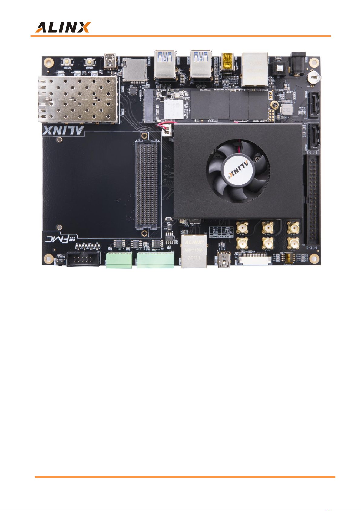
This MPSoCs FPGA development platform adopts the core board + carrier
board mode, which is convenient for users to use the core board for secondary
development. The core board uses XILINX Zynq UltraScale+ EG chip ZU15EG
solution, uses Processing System(PS)+Programmable Logic(PL) technology to
integrate dual-core ARM ARM Cortex-A53 and FPGA programmable logic on a
single chip. In addition, the PS side of the core board has 4 pieces of 1GB
high-speed DDR4 SDRAM chips, 1 piece of 8GB eMMC memory chip and 1
piece of 256Mb QSPI FLASH chip; the PL side of the core board has 2 pieces
of 1GB DDR4 SDRAM chip
In the design of carrier board, we have extended a wealth of interfaces for
users, such as 1 FMC LPC interface, 1 SATA M.2 interface, 1 DP interface, 1
PCIe x 2.0, 4 USB 3.0 Interface, 2 Gigabit Ethernet interfaces, 1 HDMI Output,
1 HDMI Input, 2 Uart, 1 SD card slot, 2-Channel CAN bus interfaces,
2-Channel RS485 bus interfaces, 1 MIPI Camera Interface. It meets users'
requirements for high-speed data exchange, data storage, Video transmission
processing, deep learning, artificial intelligence and industrial control. It is a
"professional" ZYNQ development platform. For high-speed data transmission
and exchange, pre-verification and post-application of data processing is
possible. This product is very suitable for students, engineers and other groups
engaged in MPSoCs development.
AXU15EGB User Manual
6 / 66
www.alinx.com

AXU15EGB User Manual
7 / 66
www.alinx.com
Part 1: FPGA Development Board Introduction
The entire structure of the AXU15EGB PGA development board is
inherited from our consistent core board + carrier board model. A high-speed
inter-board connector is used between the core board and the carrier board.
The core board is mainly composed of the smallest system of ZU15EG +
6 DDR4 + eMMC + 2 QSPI FLASH, the main FPGA chip is Xilinx's Zynq
UltraScale+ MPSoCs family chip, the model number is
XCZU15EG-2FFVB1156I. ZU15EG chip can be divided into processor system
part Processor System (PS) and programmable logic part Programmable Logic
(PL). On the PS side and PL side of the ZU15EG chip, there are 4 DDR4 and 2
DDR4 respectively, each with a capacity of up to 1GB, which enables the ARM
system and FPGA system to independently process and store data. The 8GB
eMMC FLASH memory chip and two 256Mb QSPI FLASH which are on the
PS side, used to statically store the operating system, file system and user data
of MPSoCs.
The AXU15EGB carrier board expands its rich peripheral interface,
including 1 M.2 interface, 1 DP output interface, 4 USB 3.0 Interface, 2 Gigabit
Ethernet interfaces, 2 SFP Interfaces, 2 SATA Interfaces, 2 UART, 1 SD card
slot, 1 FMC Interface, 2-Channel CAN bus interfaces, 2-Channel RS485 bus
interfaces, 1 MIPI Camera Interface, 40-pin expansion ports and some keys
and LEDs.
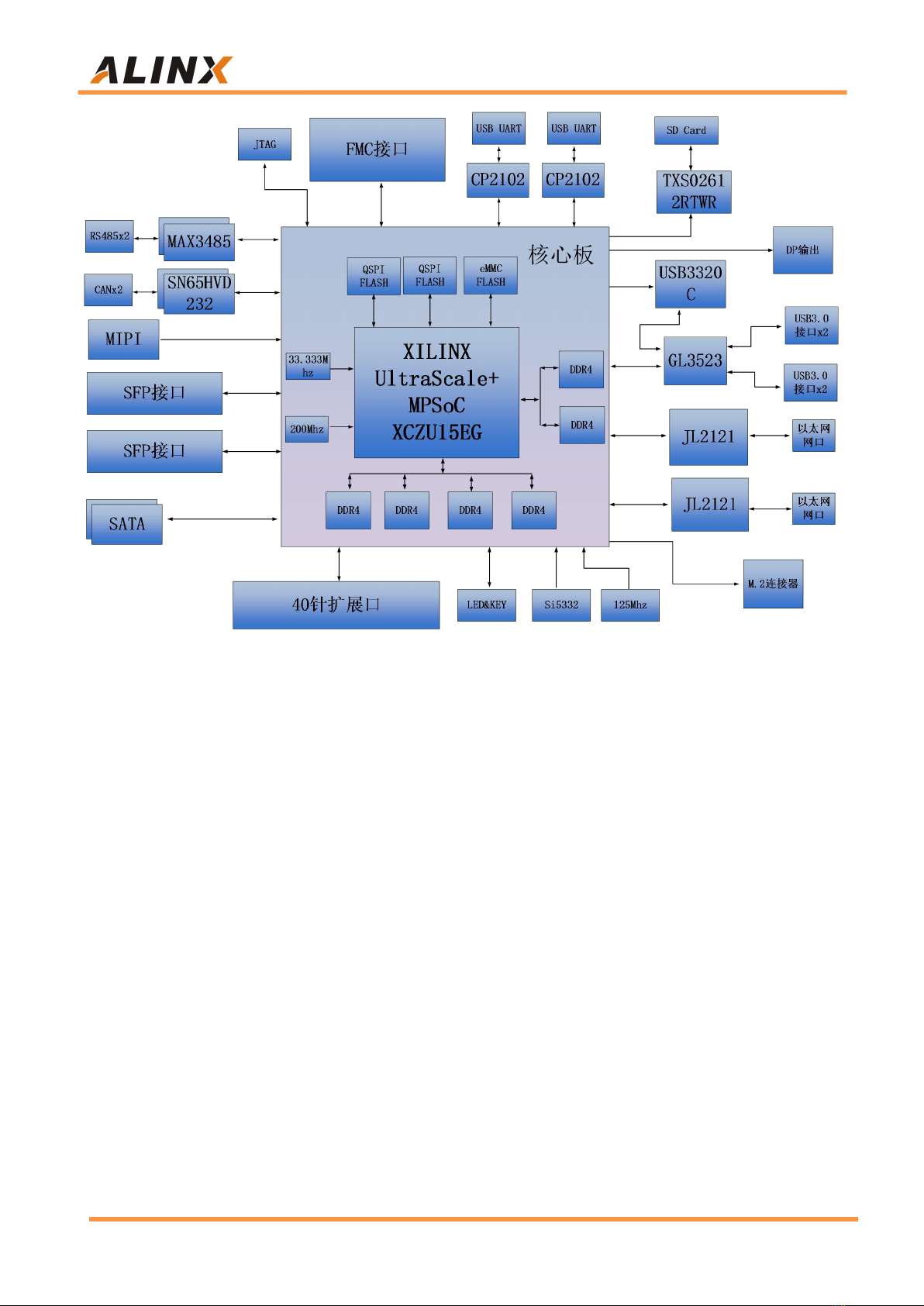
The following figure shows the structure of the entire development system:
AXU15EGB User Manual
8 / 66
www.alinx.com
Figure 1-1-1: The Schematic Diagram of the AXU15EGB
Through this diagram, you can see the interfaces and functions that the
AXU15EGB FPGA Development Board contains:
ZU15EG core board
It consists of ZU15EG +4GB DDR4(PS)+2GB DDR4(PL)+8GB eMMC
FLASH + 512Mb QSPI FLASH, and there are 2 crystal oscillators to
provide the clock, a single-ended 33.3333MHz crystal oscillator for the
PS system, and a differential 200MHz crystal oscillator for the PL logic
DDR reference clock.
M.2 Interface
1 PCIEx1 standard M.2 interface, used to connect M.2 SSD solid state
drives, with a communication speed of up to 6Gbps.
DP Output Interface

AXU15EGB User Manual
9 / 66
www.alinx.com
1 standard Display Port output display interface, used for video image
display. Supports up to 4K@30Hz or 1080P@60Hz output
USB 3.0 Interface
4-channel USB3.0 HOST interface, USB interface type is TYPE A. Used
to connect external USB peripherals, such as connecting a mouse,
keyboard, U disk, etc.
Gigabit Ethernet Interface
2-Channel 10/100M/1000M Ethernet RJ45 interface for Ethernet data
exchange with computers or other network devices. The network
interface chip uses JLSemi JL2121-N040I industrial grade GPHY chip.
USB Uart Interface
2-Channel Uart to USB interfaces for communication with the computer,
for user debugging. The serial port chip adopts the USB-UAR chip of
Silicon Labs CP2102GM, and the USB interface adopts the MINI USB
interface.
2-Channel SFP Fiber Interface
The two high-speed transceivers of the GTH transceiver are connected
to the transmitting and receiving of two optical modules, realizing two
high-speed optical fiber communication interfaces. The transmitting and
sending speed of each optical fiber data communication is as high as
12.5Gb/s.
SD Card Slot Interface
1 Micro SD card holder, used to store operating system image and file
system.
FMC Expansion Interface
1 standard FMC LPC expansion port, which can be connected to
various FMC modules of XILINX or ALINX (HDMI input and output
modules, binocular camera modules, high-speed AD modules, etc.).
CAN Communication Interface

AXU15EGB User Manual
10 / 66
www.alinx.com
Two-way CAN bus interface, using TI's SN65HVD232 chip, the
interface uses 4Pin green terminal blocks.
485 Communication Interface
Two-way 485 communication interface, using MAX3485 chip of MAXIM
company. The interface uses 6Pin green terminal blocks.
MIPI Interface
2 Lane MIPI camera input interfaces, used to connect MIPI camera
module (AN5641).
40-pin Expansion Header
The 40-pin 2.54mm pitch expansion port use for external ALINX
modules (binocular camera, TFT LCD screen, high-speed AD module,
etc.). The expansion port includes 1 channel of 5V power supply, 2
channels of 3.3V power supply, 3 channels of ground, and 34 channels
of IO port.
JTAG debug port
A 10-pin 0.1 spacing standard JTAG ports for FPGA program download
and debugging. Users can debug and download the ZU4EV system
through the XILINX downloader.
Temperature and humidity sensor chip LM75
On-board temperature and humidity sensor chip LM75, used to detect
the temperature and humidity of the surrounding environment around
the FPGA development board
EEPROM
One EEPROM 24LC04 with I2C interface
Real Time Clock (RTC)
1 built-in RTC real-time clock
LED Lights
5 LEDs, include 1 LED on the core board, 4 LEDs on the carrier board.
There are 1 power indicator and on the core board. There are 1 power
This manual suits for next models
1
Table of contents
Other Alinx Computer Hardware manuals

Alinx
Alinx ZYNQ 7000 User manual

Alinx
Alinx ARTIX-7 FPGA User manual

Alinx
Alinx ALTER AC4075 User manual

Alinx
Alinx AV6150 User manual

Alinx
Alinx UltraScale+ AXU4EV-P User manual

Alinx
Alinx AV6045 User manual

Alinx
Alinx ACU2CG User manual

Alinx
Alinx AX301 User manual

Alinx
Alinx ZYNQ AC7Z035 User manual

Alinx
Alinx KINTEX-7FPGA User manual


Popular Computer Hardware manuals by other brands

EMC2
EMC2 VNX Series Hardware Information Guide

Panasonic
Panasonic DV0PM20105 Operation manual

Mitsubishi Electric
Mitsubishi Electric Q81BD-J61BT11 user manual

Gigabyte
Gigabyte B660M DS3H AX DDR4 user manual
Raidon
Raidon iT2300 Quick installation guide

National Instruments
National Instruments PXI-8186 user manual