Nikon VAA35001 Coolpix S1 Operating instructions

作成承認印 配布許可印
Copyright c 2005 by Nikon Corporation.
All Rights Reserved.
無断転載を禁ず
!!
Printed in Japan April 2005
VAA35001-R.3666.A
REPAIR MANUAL
VAA35001

VAA35001-R.3666.A
- S1 -
CONTENTS
SPECIFICATIONS ・・・・・・・・・・・・・・・・・・・・・・・・・・・・・・・・・・・・・・・・・・・・・・・・・・・・・・・・・・・・・・・・・・・・・・・・・M1-M2
DISASSEMBLY
WARNING・・・・・・・・・・・・・・・・・・・・・・・・・・・・・・・・・・・・・・・・・・・・・・・・・・・・・・・・・・・・・・・・・・・・・・・・・・・・・・・・・・D1
REAR COVER ・・・・・・・・・・・・・・・・・・・・・・・・・・・・・・・・・・・・・・・・・・・・・・・・・・・・・・・・・・・・・・・・・・・・・・・・・・・・・・D2
LCD ・・・・・・・・・・・・・・・・・・・・・・・・・・・・・・・・・・・・・・・・・・・・・・・・・・・・・・・・・・・・・・・・・・・・・・・・・・・・・・・・・・・・・・・D3
MONITOR HOLDER ・・・・・・・・・・・・・・・・・・・・・・・・・・・・・・・・・・・・・・・・・・・・・・・・・・・・・・・・・・・・・・・・・・・・・・・・・D4
CARD HOLDER ・・・・・・・・・・・・・・・・・・・・・・・・・・・・・・・・・・・・・・・・・・・・・・・・・・・・・・・・・・・・・・・・・・・・・・・・・・・・・D5
DISCHARGE OF MAIN CONDENSER ・・・・・・・・・・・・・・・・・・・・・・・・・・・・・・・・・・・・・・・・・・・・・・・・・・・・・・・・・・ D6
PLACE WHICH MUST NOT BE TOUCHED IN LENS UNIT・・・・・・・・・・・・・・・・・・・・・・・・・・・・・・・・・・・・・・・・・D7
FRONT COVER ・・・・・・・・・・・・・・・・・・・・・・・・・・・・・・・・・・・・・・・・・・・・・・・・・・・・・・・・・・・・・・・・・・・・・・・・・・・・・ D7
STAND・・・・・・・・・・・・・・・・・・・・・・・・・・・・・・・・・・・・・・・・・・・・・・・・・・・・・・・・・・・・・・・・・・・・・・・・・・・・・・・・・・・・・D8
BARRIER MOTOR UNIT ・・・・・・・・・・・・・・・・・・・・・・・・・・・・・・・・・・・・・・・・・・・・・・・・・・・・・・・・・・・・・・・・・・・・・D9
BATTERY HOLDER・・・・・・・・・・・・・・・・・・・・・・・・・・・・・・・・・・・・・・・・・・・・・・・・・・・・・・・・・・・・・・・・・・・・・・・・ D10
CONTROL TOP UNIT ・・・・・・・・・・・・・・・・・・・・・・・・・・・・・・・・・・・・・・・・・・・・・・・・・・・・・・・・・・・・・・・・・・・・・・D10
SPEAKER/MICROPHONE ・・・・・・・・・・・・・・・・・・・・・・・・・・・・・・・・・・・・・・・・・・・・・・・・・・・・・・・・・・・・・・・・・・D11
MAIN PCB UNIT CP-1・・・・・・・・・・・・・・・・・・・・・・・・・・・・・・・・・・・・・・・・・・・・・・・・・・・・・・・・・・・・・・・・・・・・・・D12
LED PCB UNIT TB-1・・・・・・・・・・・・・・・・・・・・・・・・・・・・・・・・・・・・・・・・・・・・・・・・・・・・・・・・・・・・・・・・・・・・・・・D13
FLASH UNIT ・・・・・・・・・・・・・・・・・・・・・・・・・・・・・・・・・・・・・・・・・・・・・・・・・・・・・・・・・・・・・・・・・・・・・・・・・・・・・D13
ASSEMBLY
FLASH UNIT ・・・・・・・・・・・・・・・・・・・・・・・・・・・・・・・・・・・・・・・・・・・・・・・・・・・・・・・・・・・・・・・・・・・・・・・・・・・・・・・A1
PLACE WHICH MUST NOT BE TOUCHED IN LENS UNIT・・・・・・・・・・・・・・・・・・・・・・・・・・・・・・・・・・・・・・・・・A2
LED PCB UNIT TB-1・・・・・・・・・・・・・・・・・・・・・・・・・・・・・・・・・・・・・・・・・・・・・・・・・・・・・・・・・・・・・・・・・・・・・・・・・A2
MAIN PCB UNIT CP-1・・・・・・・・・・・・・・・・・・・・・・・・・・・・・・・・・・・・・・・・・・・・・・・・・・・・・・・・・・・・・・・・・・・・・・・・A3
SPEAKER/MICROPHONE ・・・・・・・・・・・・・・・・・・・・・・・・・・・・・・・・・・・・・・・・・・・・・・・・・・・・・・・・・・・・・・・・・・・・A4
CONTROL TOP UNIT ・・・・・・・・・・・・・・・・・・・・・・・・・・・・・・・・・・・・・・・・・・・・・・・・・・・・・・・・・・・・・・・・・・・・・・・・A5
ASSEMBLY OF BATTERY HOLDER・・・・・・・・・・・・・・・・・・・・・・・・・・・・・・・・・・・・・・・・・・・・・・・・・・・・・・・・・・・・A6
BATTERY HOLDER・・・・・・・・・・・・・・・・・・・・・・・・・・・・・・・・・・・・・・・・・・・・・・・・・・・・・・・・・・・・・・・・・・・・・・・・・・ A7
BARRIER MOTOR UNIT ・・・・・・・・・・・・・・・・・・・・・・・・・・・・・・・・・・・・・・・・・・・・・・・・・・・・・・・・・・・・・・・・・・・・・A8
STAND・・・・・・・・・・・・・・・・・・・・・・・・・・・・・・・・・・・・・・・・・・・・・・・・・・・・・・・・・・・・・・・・・・・・・・・・・・・・・・・・・・・・・A9
FRONT COVER ・・・・・・・・・・・・・・・・・・・・・・・・・・・・・・・・・・・・・・・・・・・・・・・・・・・・・・・・・・・・・・・・・・・・・・・・・・・ A10
ASSEMBLY OF CARD HOLDER ・・・・・・・・・・・・・・・・・・・・・・・・・・・・・・・・・・・・・・・・・・・・・・・・・・・・・・・・・・・・・A11
CARD HOLDER ・・・・・・・・・・・・・・・・・・・・・・・・・・・・・・・・・・・・・・・・・・・・・・・・・・・・・・・・・・・・・・・・・・・・・・・・・・・A12
MONITOR HOLDER ・・・・・・・・・・・・・・・・・・・・・・・・・・・・・・・・・・・・・・・・・・・・・・・・・・・・・・・・・・・・・・・・・・・・・・・A13
LCD ・・・・・・・・・・・・・・・・・・・・・・・・・・・・・・・・・・・・・・・・・・・・・・・・・・・・・・・・・・・・・・・・・・・・・・・・・・・・・・・・・・・・・A14
REAR COVER ・・・・・・・・・・・・・・・・・・・・・・・・・・・・・・・・・・・・・・・・・・・・・・・・・・・・・・・・・・・・・・・・・・・・・・・・・・・・A15

VAA35001-R.3666.A
- S1 -
ADJUSTMENT ・・・・・・・・・・・・・・・・・・・・・・・・・・・・・・・・・・・・・・・・・・・・・・・・・・・・・・・・・・・・・・・・・・・・A16-A26
DESCRIPTION OF CIRCUIT ・・・・・・・・・・・・・・・・・・・・・・・・・・・・・・・・・・・・・・・・・・・・・・・・・・・・・・・・・・・・・・・・E1-E8
ELECTRICITY
OVERALL WIRING ・・・・・・・・・・・・・・・・・・・・・・・・・・・・・・・・・・・・・・・・・・・・・・・・・・・・・・・・・・・・・・・・・・・・・・・・・・E9
CP1(DMA) CIRCUIT DIAGRAM ・・・・・・・・・・・・・・・・・・・・・・・・・・・・・・・・・・・・・・・・・・・・・・・・・・・・・・・・・・・・・E10
CP1(SYA) CIRCUIT DIAGRAM ・・・・・・・・・・・・・・・・・・・・・・・・・・・・・・・・・・・・・・・・・・・・・・・・・・・・・・・・・・・・・・E11
CP1(PWA) CIRCUIT DIAGRAM・・・・・・・・・・・・・・・・・・・・・・・・・・・・・・・・・・・・・・・・・・・・・・・・・・・・・・・・・・・・・・E12
CP1(STA) CIRCUIT DIAGRAM ・・・・・・・・・・・・・・・・・・・・・・・・・・・・・・・・・・・・・・・・・・・・・・・・・・・・・・・・・・・・・・ E13
TB1 CIRCUIT DIAGRAM ・・・・・・・・・・・・・・・・・・・・・・・・・・・・・・・・・・・・・・・・・・・・・・・・・・・・・・・・・・・・・・・・・・・E14
CA1 CIRCUIT DIAGRAM ・・・・・・・・・・・・・・・・・・・・・・・・・・・・・・・・・・・・・・・・・・・・・・・・・・・・・・・・・・・・・・・・・・・E15
OVERALL BLOCK DIAGRAM・・・・・・・・・・・・・・・・・・・・・・・・・・・・・・・・・・・・・・・・・・・・・・・・・・・・・・・・・・・・・・・E16
ASIC BLOCK DIAGRAM ・・・・・・・・・・・・・・・・・・・・・・・・・・・・・・・・・・・・・・・・・・・・・・・・・・・・・・・・・・・・・・・・・・・E17
CCD BLOCK DIAGRAM・・・・・・・・・・・・・・・・・・・・・・・・・・・・・・・・・・・・・・・・・・・・・・・・・・・・・・・・・・・・・・・・・・・・E18
LENS BLOCK DIAGRAM ・・・・・・・・・・・・・・・・・・・・・・・・・・・・・・・・・・・・・・・・・・・・・・・・・・・・・・・・・・・・・・・・・・・E19
SYSTEM CONTROL BLOCK DIAGRAM ・・・・・・・・・・・・・・・・・・・・・・・・・・・・・・・・・・・・・・・・・・・・・・・・・・・・・・E20
POWER BLOCK DIAGRAM ・・・・・・・・・・・・・・・・・・・・・・・・・・・・・・・・・・・・・・・・・・・・・・・・・・・・・・・・・・・・・・・・・E21
FUSE ARRANGEMENT (CP1 PCB) ・・・・・・・・・・・・・・・・・・・・・・・・・・・・・・・・・・・・・・・・・・・・・・・・・・・・・・・・・・・E22
INSPECTION STANDARDS ・・・・・・・・・・・・・・・・・・・・・・・・・・・・・・・・・・・・・・・・・・・・・・・・・・・・・・・・・・・・・・ R1-R10
TOOL LIST・・・・・・・・・・・・・・・・・・・・・・・・・・・・・・・・・・・・・・・・・・・・・・・・・・・・・・・・・・・・・・・・・・・・・・・・・・・・・・・T1-T2

VAA35001-R.3666.A
- M1・ S1 -
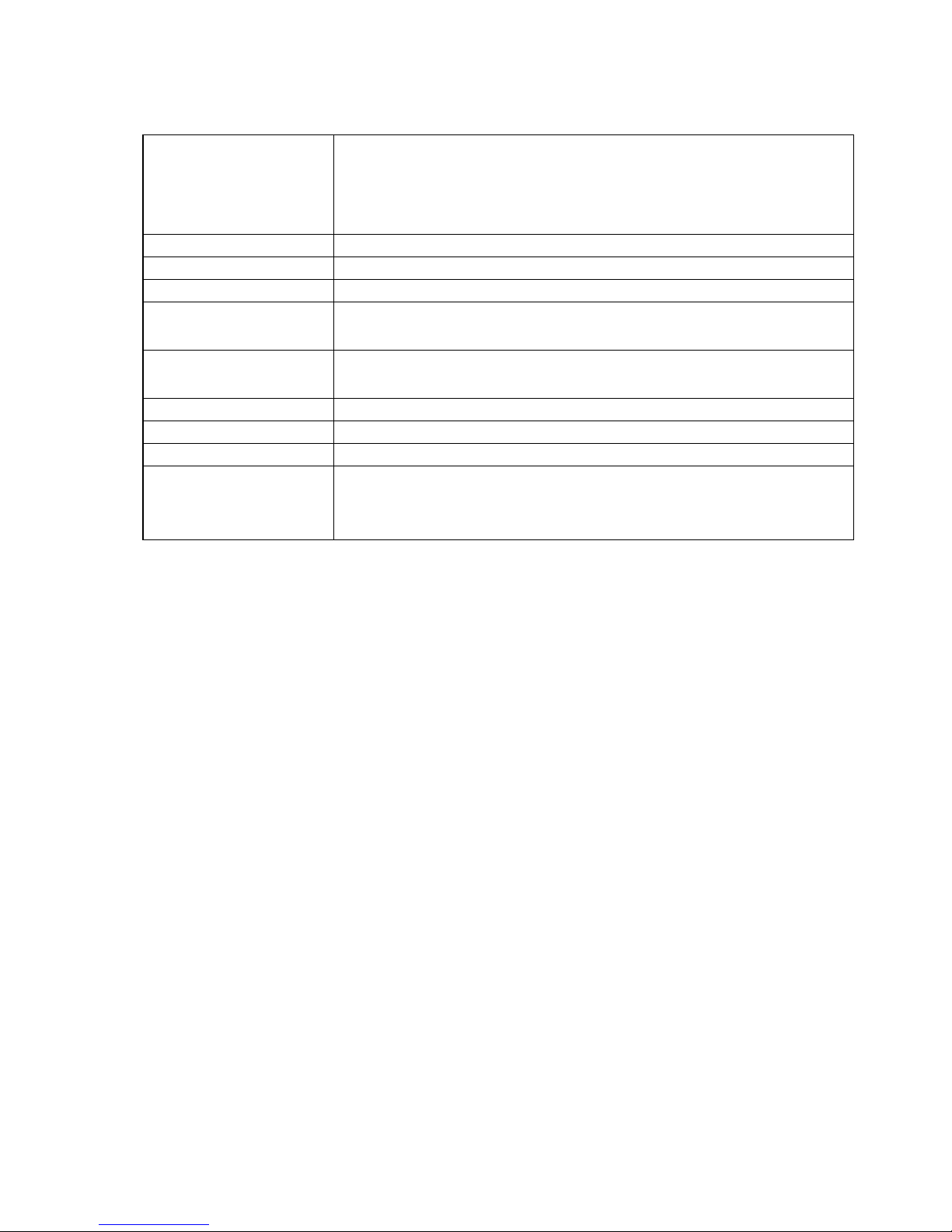
Type COOLPIX S1 digital camera
Effective pixels 5.1 million
CCD
Image size (pixels)
1/2.5” CCD; total pixels: 5.36 million
2,592 × 1,944 (2592*, 2592)
2,048 × 1,536 (2048)
1,024 × 768 (1024)
640 × 480 (640)
Lens
Focal length
f/-number
Construction
3 × Zoom Nikkor ED lens
F=5.8 - 17.4 mm
(35-mm [135] camera-format equivalent: 35 - 105 mm)
f/3.0 - f/5.4
12 elements in 10 groups
Digital zoom Up to 4 × (35-mm [135] camera-format equivalent:420 mm)
Autofocus (AF)
Focus range
(distance from lens)
Focus-area selection
AF-assist illuminator
Contrast-detect through the lens (TTL) AF, with AF-assist illuminator
30 cm (1') - ∞
Macro mode: 4 cm(1.6”) - ∞ (middle zoom position)
Center; auto multi AF
Class 1 LED product (IEC60825-1 Edition 1.2-2001)
Max. output: 2,000 μW
Monitor
Approximate frame
coverage
2.5”, 110,000-dot, TFT LCD monitor, brightness adjustment (5 step)
Shooting mode: 97% horizontal and 97% vertical
Playback: 100% horizontal and 100% vertical
Storage Media
File system
File formats
Internal memory (approx.12 MB); SD (Secure Digital) memory cards
Compliant with Design Rule for Camera File System (DCF)*, Exif 2.2+, and Digital
Print Order Format (DPOF)
Compressed: JPEG-baseline-compliant
Movies: QuickTime
Sound les: WAV
Exposure
Metering
Exposure control
Range
256-segment matrix metering linked to AF area
Programmed auto exposure with exposure compensation
(-2.0 - +2.0 EV in steps of 1/3 EV)
W: +1.2 - +15.2 EV
T: +2.9 - +17.3 EV
Shutter
Speed
Mechanical and charge-coupled electronic shutter
2 - 1/350 s
Aperture
Range
Electronically-controlled ND- lter selection
2 steps (f/3.0 and f/8.5 [W])
Sensitivity Approximately equivalent to ISO 50, 100, 200, 400; Auto
Self-timer Approximately 10 seconds
SPECIFICATIONS
VAA35001-R.3666.A
- M2・ S1 -
Built-in ash
Range (approx.)
Sync method
W: 0.3 - 2.5 m/1' - 8'2”
T: 0.3 - 1.4 m/1' - 4'7”
Sensor ash system
Interface USB
Video output NTSC, PAL
I/O terminals Multi connector
Supported languages Chinese (Simpli ed and Traditional), Dutch, English, French, German, Italian, Japanese,
Korean, Russian, Spanish, Swedish
Power sources ・One rechargeable Nikon EN-EL8 lithium-ion battery (supplied)
・EH-63 AC adapter (supplied)
Battery life Approx. 200 shots (EN-EL8; based on CIPA standard *)
Dimensions (W × H × D) 89.9 × 57.5 × 19.7 mm/3.5”× 2.3”× 0.8”(W × H × D)
Approximate weight 118 g (4 oz) without battery or memory card
Operating environment
Temperature
Humidity
0 - 40 ℃ (32 - 104°F )
Less than 85% (no condensation)
* Industry standard for measuring life of camera batteries. Measured at 25 °C (77 °F); zoom adjusted with each shot,
ash red with every other shot, image mode set to NORMAL.
All gures are for a camera with a fully-charged EN-EL8 battery operated at an ambient temperature of 25 °C (77 °F).

VAA35001-R.3666.A
- D1・ S1 -
DISASSEMBLY
Points to notice for Lead-free solder products
・ Lead-free solder is used for this product.
・ For soldering work, the special solder and soldering iron are required.
・ Do NOT mix up lead-free solder with traditional solder.
・ Use the special soldering iron respectively for lead-free solder and lead solder. They cannot
be used in common.
Note : ① Before disassembling, remove the SD card and the charged battery.
② When disassembling, make sure to memorize the processing state of wires, screws to be
xed and their types, etc.
③ Because electrical parts are easily damaged by static electricity, make sure that you are
well earthed/grounded.

VAA35001-R.3666.A
- D2・ S1 -
REAR COVER
・ Remove 2 screws [#101]. ・ Remove 4 screws [#102].
・ Remove 4 screws [#102]. ・ Unhook the rear cover [#029] and open the rear cover
[#029].
・ Remove the FPC from the connector.
Screw [#102]
Screw [#102]
Screw [#102]
Screw [#102]
Screw [#101]
FPC
Rear cover [#029]
Hook

VAA35001-R.3666.A
- D3・ S1 -
LCD
・ Unhook and lift up the LCD [#008].
・ Remove the connector and the FPC.
Hook
Hook
LCD [#008]
Connector
FPC

VAA35001-R.3666.A
- D4・ S1 -
MONITOR HOLDER
・ Remove the bosses from the side ornament [#002] and pull it out in the arrow direction.
Screw [#103]
Strap shaft [#018]
Monitor holder [#001]
Boss
・ Remove 2 screws [#103].
・ Remove the monitor holder [#001].
・ Remove the strap shaft [#018].
Monitor holder [#001]
Side ornament [#002]
Boss

VAA35001-R.3666.A
- D5・ S1 -
CARD HOLDER
・ Pull out the card holder [#014] in the arrow direction.
Card holder [#014]
This manual suits for next models
2
Table of contents
Other Nikon Digital Camera manuals

Nikon
Nikon COOLPIX AW100 User manual

Nikon
Nikon D60 User manual

Nikon
Nikon Coolpix S810c User manual

Nikon
Nikon D200 User manual

Nikon
Nikon CoolPix S560 User guide

Nikon
Nikon COOLPIX 570 User manual

Nikon
Nikon D80 User manual

Nikon
Nikon D500 Service manual

Nikon
Nikon 1 v3 User manual

Nikon
Nikon Coolpix S6100 User manual

Nikon
Nikon CoolPix 800 User manual

Nikon
Nikon D5300 User manual

Nikon
Nikon COOLPIX L1 User manual

Nikon
Nikon Coolpix S4100 User manual

Nikon
Nikon D200 User manual

Nikon
Nikon D60 User manual

Nikon
Nikon Coolpix L32 User manual

Nikon
Nikon 25480 User manual

Nikon
Nikon N50 User manual

Nikon
Nikon CoolPix S2 User manual


