Crystal Clear T700T09X00 Owner's manual

Product Specification
T700T09X00
(REVISION 5)
Crystal Clear Technology Sdn. Bhd.
16 Jalan TP5, Taman Perindustrian Sime UEP,
47600 Subang Jaya, Selangor DE
Tel: 603-80247099
Website: www.cct.com.my
CRYSTAL CLEAR TECHNOLOGY SDN BHD
Spec. No: T700T09X00 REV5
1
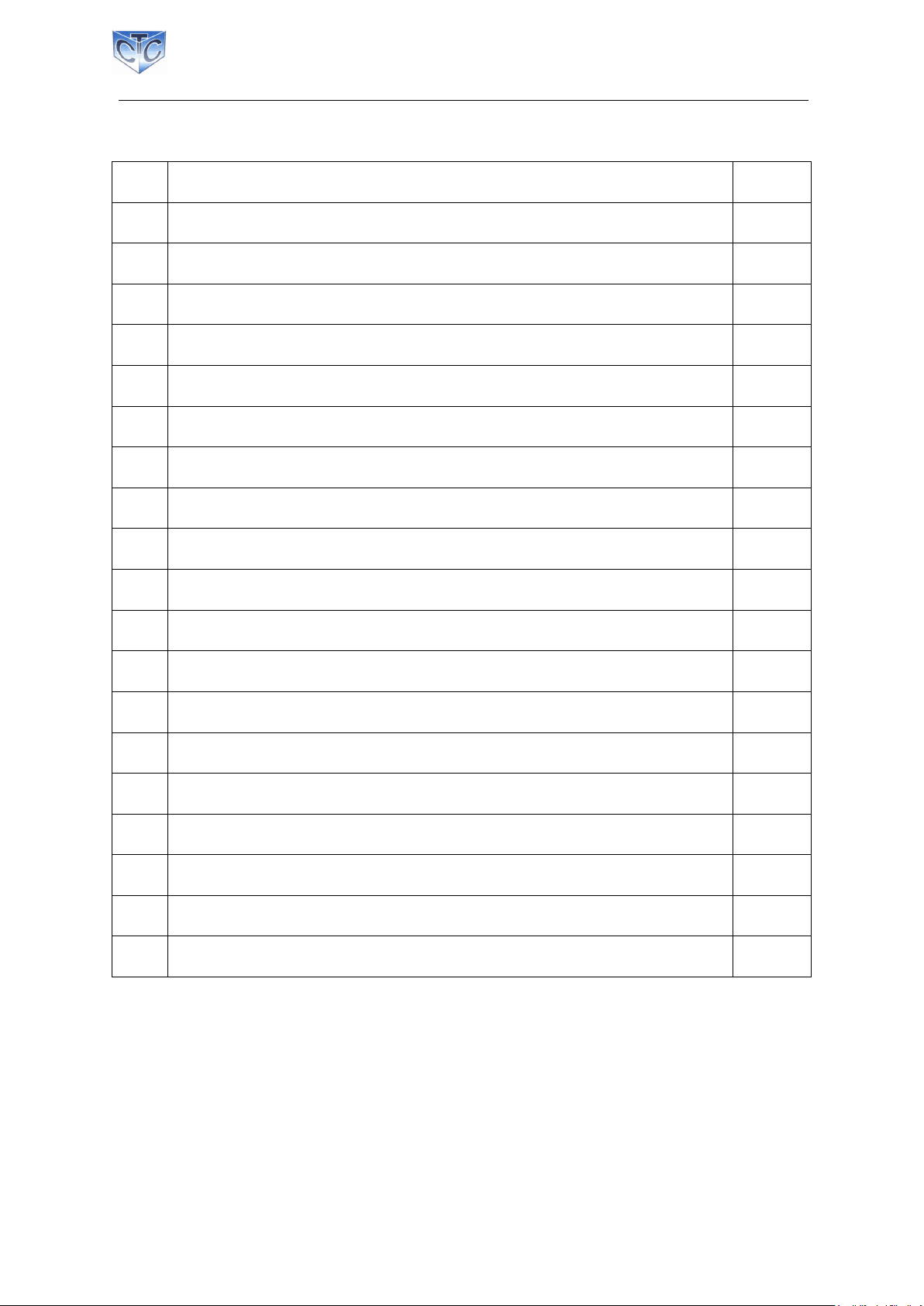
1.0 Table of Contents
No Title Page
1 Table of Contents 1
2 Record of revision 2
3 General Specification 3
4 Absol te Maxim m Ratings 4
5 Electrical Characteristics 5
6 Pin Assignment 7
7 Optical Characteristics 9
8 Timing Characteristics 12
9 Reliability Test Condition 14
10 Inspection Criteria 15
11 Preca tion and Limited Warranty 16
12 Mechanical Specification 20
13 Attachment:
Capacitive To ch Panel Specification – TP0085
CRYSTAL CLEAR TECHNOLOGY SDN BHD
Spec. No: T700T09X00 REV5
2
2.0 Records of Revision
Rev
Date
Item
Page
Comment
Originator
Checked By
1.0
2.0
3.0
4.0
5.0
22.11.15
08.12.15
28.01.16
01.03.16
10.05.16
Initial Release
Update mechanical drawing
Change IC
Change model name T700B09N00 to
T700X09X00
Change viewing direction
Change model name T700X09X00 to
T700T09X00, update reliability test,
change inspection criteria, change
precaution and limited warranty.
Azhar
Azhar
Azhar
Azhar
Adam
Liew
Liew
Azhar
Azhar
Azhar
CRYSTAL CLEAR TECHNOLOGY SDN BHD
Spec. No: T700T09X00 REV5
3
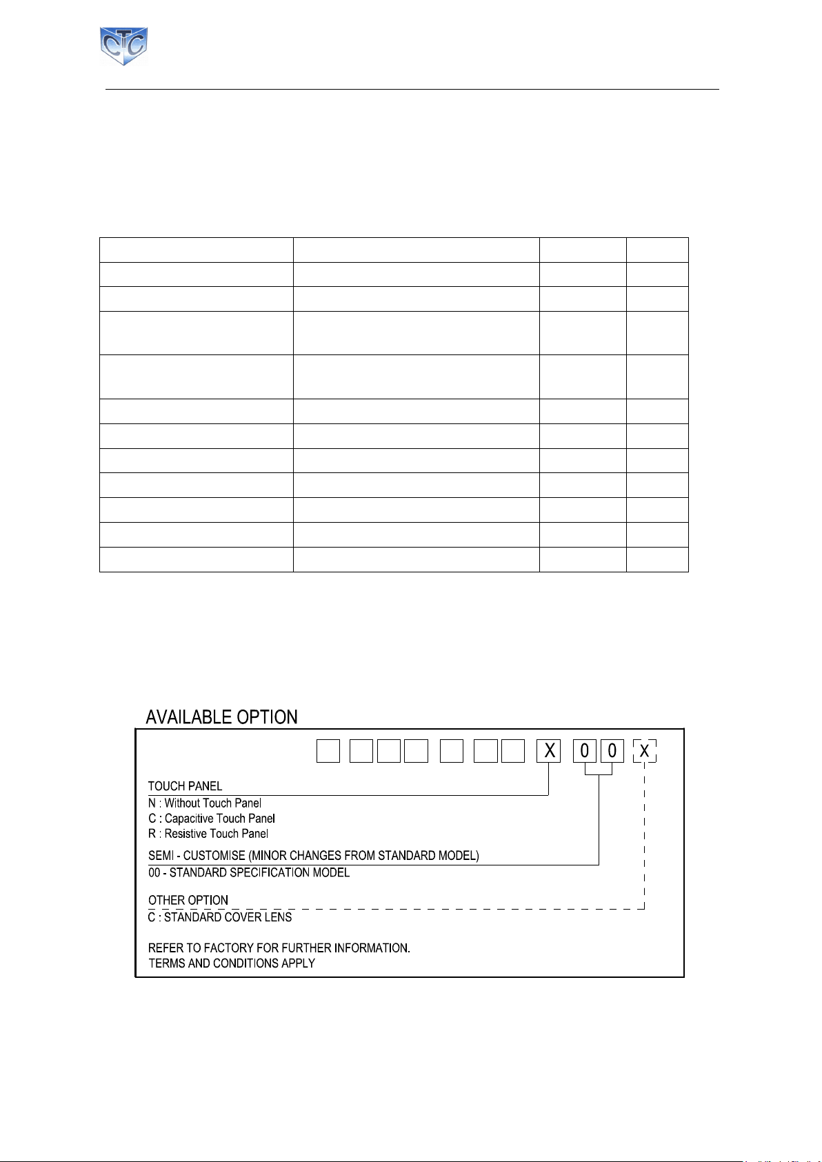
3.0 General Specification
T700T09X00 is 7.0” color TFT-LCD (Thin Film Transistor Liq id Crystal Display)
mod le composed of LCD panel, driver ICs control circ it, LED backlight. This display area
contains 1024 x 600 pixels and can display p to 16M colors. This prod ct compliant
with RoHS environmental req irement.
Item Contents Unit Note
LCD Type 7.0” TFT -
Display color 16M 1
Viewing Direction
(Optim m View) 12 O ’Clock
Viewing Direction
(Grey Inversion) 6 O ’Clock
Mod le size 165.4 X 105.7 X 2.78 mm 2
Active Area(W×H) 153.6 X 90.0 mm
N mber of Dots 1024×RGB×600 dots
Driver IC NT51008CH/NT52002H -
Backlight 27 White LEDs pcs
Brightness 500 (TYP) cd/m2
Interface Mode LVDS -
Note1: Color tone is slightly changed by temperat re and driving voltage.
Note2: FPC or wire are not incl ded.
Note3: Brightness on LCD s rface. Mod le with CTP or RTP, brightness will be abo t
20% (max) lower on the to ch panel s rface.
CRYSTAL CLEAR TECHNOLOGY SDN BHD
Spec. No: T700T09X00 REV5
4
4.0 Absol te Maxim m Ratings
4.1 Electrical Absol te Maxim m ratings (Vss = 0V, Ta = 25°C)
Item Symbol Min. Max. Unit Note
Power Voltage
DVDD -0.3 5.0 V
AVDD 6.5 13.5 V
VGH -0.3 42.0 V
VGL -20.0 0.3 V
VGH-VGL 40.0 V
Notes:
1.
If the mod le is above these absol te maxim m ratings. It may become
permanently damaged.
2.
VR Condition: Zener Diode: 20mA.
3.
Please be s re sers are gro nded when handing LCD Mod le.
4 2 Environmental Absolute Maximum Ratings
Item
Storage Operating
Note
MIN. MAX. MIN. MAX.
Ambient Temperat re -30
℃
70
℃
-20
℃
60
℃
1,2
H midity - - - - 3
1.
The response time will become lower when operated at low temperat re.
2.
Backgro nd color changes slightly depending on ambient temperat re. The
phenomenon is reversible.
3.
Ta<=40°C and 85%RH MAX.
(Ta>=40°C. Absol te h midity m st be lower than the h midity of 85%RH at
40°C)
CRYSTAL CLEAR TECHNOLOGY SDN BHD
Spec. No: T700T09X00 REV5
5
5.0 Electrical Characteristics and Instr ction Code
5.1 Electrical Characteristics (Vss = 0V, Ta = 25°C)
Parameter Symbol Min Typ Max Unit Note
Power s pply
DVDD 3.0 3.3 3.6 V Note 2
AVDD 10.8 11 11.2 V
VGH 19.7 20 20.3 V
VGL -6.5 -6.8 -7.1 V
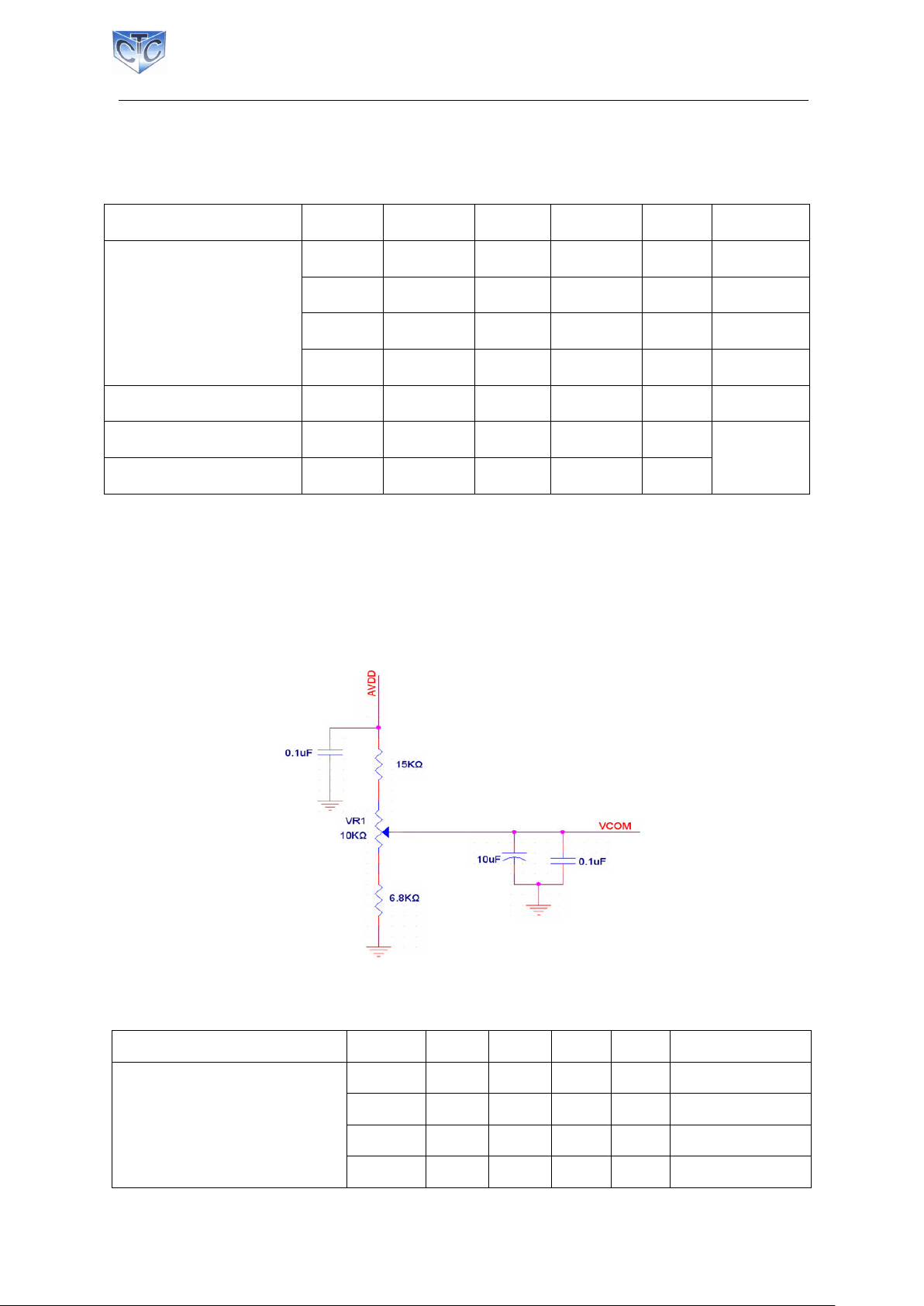
Inp t signal voltage VCOM 2.8 (3.8) 4.8 V
Inp t logic high voltage VIH 0.7DVDD
- DVDD V
Note 3
Inp t logic low voltage VIL 0 - 0.3DVDD
V
Note 1: DVDD and VGL m st be applied first before we can apply VGH.
Note 2: DVDD setting sho ld match the signals o tp t voltage (refer to Note 3) of
c stomer’s system board.
Note 3: DCLK,HS,VS,RESET,U/D, L/R,DE,R0~R7,G0~G7,B0~B7,MODE,DITHB.
Note 4: VCOM (typ) is only a reference val e, it m st be adj sted ( se VR) and
optimized on each LCM.
5.2 C rrent Cons mption
Item Symbol
Min Typ Max Unit remarks
C rrent for Driver
IGH - 0.2 1 mA VGH = 18.0V
IGL - 0.2 1 mA VGL = -6.0V
IDVDD
- 50 60 mA DVDD = 3.3V
IAVDD - 25 30 mA AVDD = 9.6V
CRYSTAL CLEAR TECHNOLOGY SDN BHD
Spec. No: T700T09X00 REV5
6
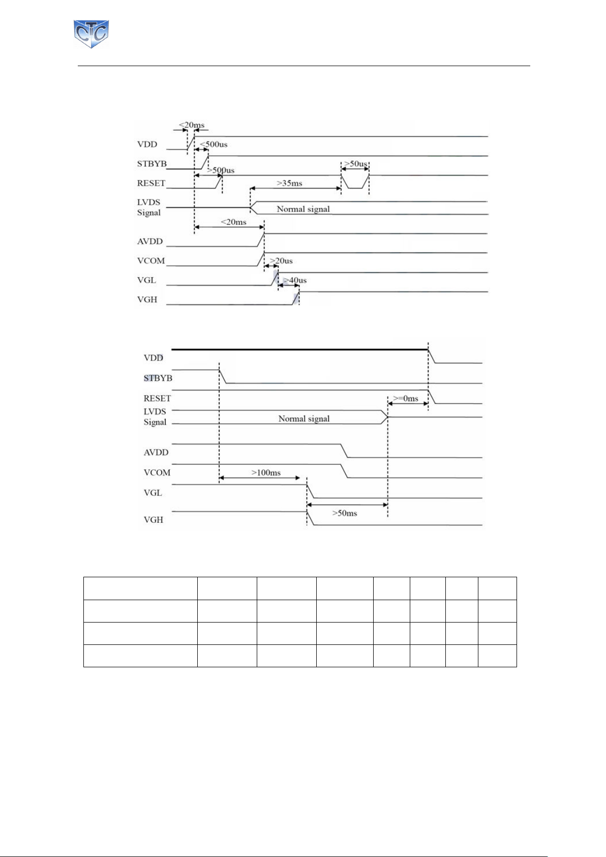
5.3 Power Seq ence
a. Power On
b. Power Off
5.4 LED Backlight Specification (Vss = 0V, Ta = 25°C)
Note:
1.
V
LED
=V
LED
(+)-V
LED
(-).
2.
It is recommended that c stomer s pply constant c rrent to prolong the led
lifetime and optim m led performance
3.
Definition of Lifetime: L minance < 50% of initial L minance
(Test condition: Ta = 25⁰C, Constant c rrent s pply (typical Val e))
Item Symbol Condition
Min Typ Max Unit
Note
S pply Voltage V
LED
- - 9.6 10.2 V 1
S pply C rrent If - - 160 170 mA
Led lifetime 20000 2
CRYSTAL CLEAR TECHNOLOGY SDN BHD
Spec. No: T700T09X00 REV5
7
6.0 Pin Assignment
P
i
n
N
o.
S
y
m
bo
l
I
/
O
F
n
ct
i
on
R
e
m
a
rk
1
VCOM P Common Voltage
2
VDD P Power Voltage for digital circ it
3
VDD P Power Voltage for digital circ it
4
NC --- No connection
5
Reset I Global reset pin
6
STBYB I
Standby mode, Normally p lled high STBYB =
“1”, normal operation STBYB = “0”, timing
controller, so rce driver will t rn off, all o tp t
are High-Z
7
GND P Gro nd
8
RXIN0- I -LVDS differential data inp t
9
RXIN0+ I + LVDS differential data inp t
10
GND P Gro nd
11
RXIN1- I -LVDS differential data inp t
12
RXIN1+ I + LVDS differential data inp t
13
GND P Gro nd
14
RXIN2- I -LVDS differential data inp t
15
RXIN2+ I + LVDS differential data inp t
16
GND P Gro nd
17
RXCLKIN- I -LVDS differential clock inp t
18
RXCLKIN+
I + LVDS differential clock inp t
19
GND P Gro nd
20
RXIN3- I -LVDS differential data inp t
21
RXIN3+ I + LVDS differential data inp t
22
GND P Gro nd
23
NC --- No connection
24
NC --- No connection
25
GND P Gro nd
26
NC --- No connection
27
DIMO O Backlight CABC controller signal o tp t
28
SELB I 6bit/8bit mode select Note1
29
AVDD P Power for Analog Circ it
30
GND P Gro nd
31
LED- P LED Cathode
CRYSTAL CLEAR TECHNOLOGY SDN BHD
Spec. No: T700T09X00 REV5
8
32
LED- P LED Cathode
33
L/R I Horizontal inversion Note3
34
U/D I Vertical inversion Note3
35
VGL P Gate OFF Voltage
36
CABCEN1
I CABC H/W enable Note2
37
CABCEN0
I CABC H/W enable Note2
38
VGH P Gate ON Voltage
39
LED+ P LED Anode
40
LED+ P LED Anode
I: inp t, O: o tp t, P: Power
Note1: If LVDS inp t data is 6 bits, SELB m st be set to High;
If LVDS inp t data is 8 bits, SELB m st be set to Low.
Note2: When CABC_EN=”00”, CABC OFF.
When CABC_EN=”01”, ser interface image.
When CABC_EN=”10”, still pict re.
When CABC_EN=”11”, moving image.
When CABC off, don’t connect DIMO, else connect it to backlight.
Note3: When L/R=”0”, set right to left scan direction.
When L/R=”1”, set left to right scan direction.
When U/D=”0”, set top to bottom scan direction.
When U/D=”1”, set bottom to top scan direction.
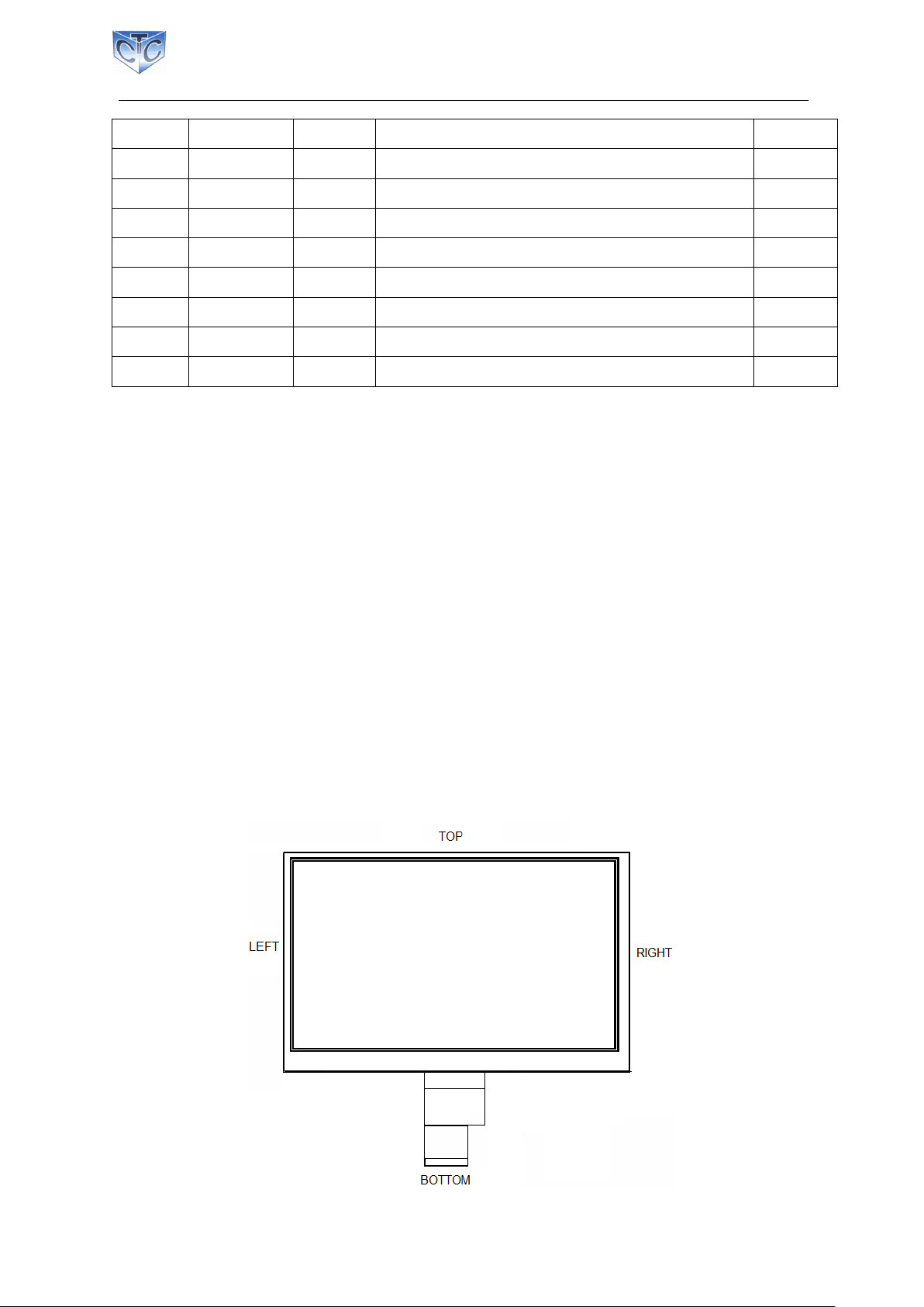
Note: Refer below fig re for Definition of scanning direction.
CRYSTAL CLEAR TECHNOLOGY SDN BHD
Spec. No: T700T09X00 REV5
9
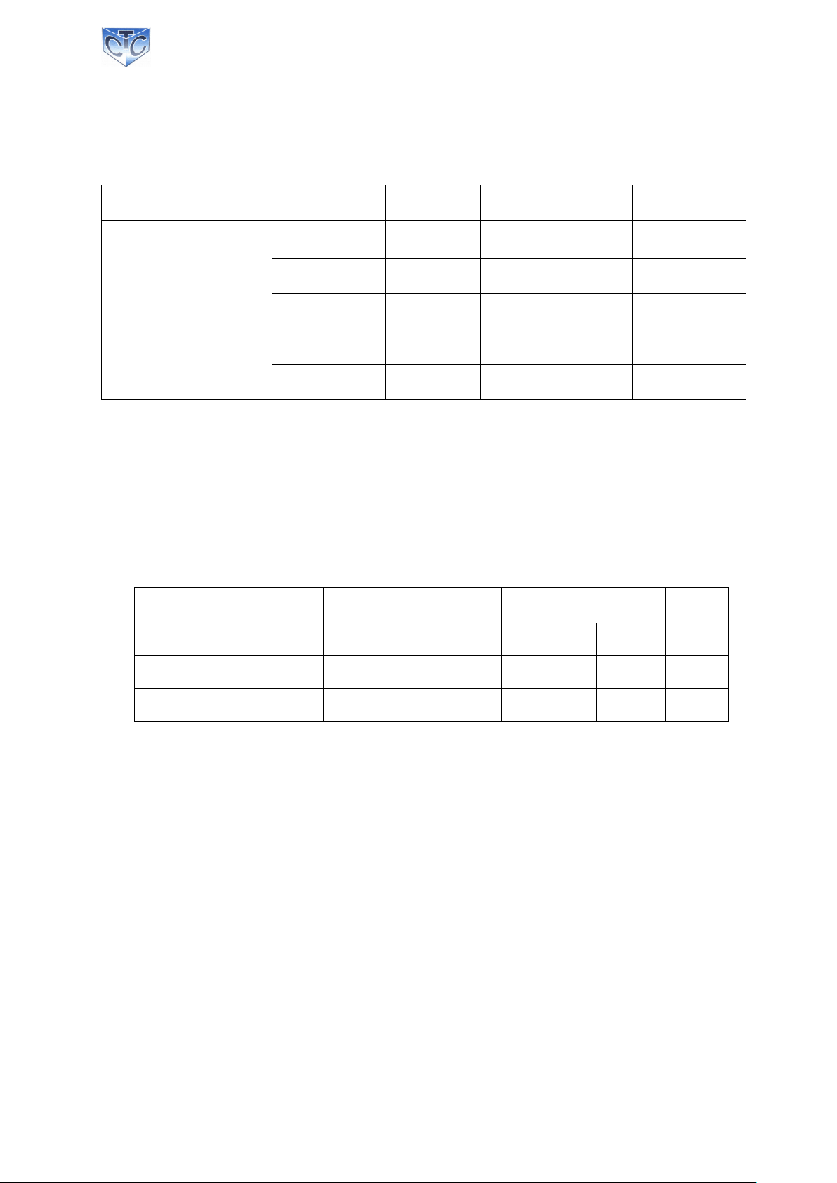
7.0 Electrical Characteristics
Items Symbol Condition Min Typ Max
Unit Remark
Response Time Tr + Tf
Θ = 0°
Ø = 0°
Ta = 25°C
- 25 50 ms Note5
Contrast Ratio Cr 500 700 - - Note4
Uniformity Δ
White - 70 - % Note2
S rface L minance Lv 300 320 - cd/m2 Note1
Viewing Angle
Θ
T
= 90
CR>10
60 70 -
° Note3
Θ
B
= 270
65 75 -
Θ
R
= 0
65 75 -
θ
L
= 180
65 75 -
CIE (X, Y)
Chromaticity
White X
W
Θ = 0°
Ø = 0°
Ta = 25°C
0.26 0.29 0.30
-
Note6
Y
W
0.26 0.29 0.30 -
Red
X
R
0.648
0.663 0.678
-
Y
R
0.310
0.325 0.340
-
Green
X
G
0.259
0.274 0.287
-
Y
G
0.587
0.602 0.617
-
Bl e
X
B
0.119
0.134 0.149
-
Y
B
0.103
0.118 0.133
-
Note: The parameter is slightly changed by temperat re, driving voltage and materiel
Note 1: The data are meas red after LEDs are t rned on for 5 min tes. LCM displays f ll white.
The brightness is the average val e of 9 meas red spots. Meas rement eq ipment
PR-705 (Φ8mm)
Meas ring condition:
- Meas ring s rro ndings: Dark room.
- Meas ring temperat re: Ta=25℃.
- Adj st operating voltage to get optim m contrast at the center of the display.
Meas red val e at the center point of LCD panel after more than 5 min tes while backlight t rning
on.
Table of contents


