
AkitikA GT-101 STEREO User manual

Page 1 of 44
GT-101 STEREO
AUDIO POWER AMPLIFIER
ASSEMBLY MANUAL
© 2013 AkitikA LLC
All rights reserved
Revision 1p37 Octo er 29, 2013

Page 2 of 44
Table of Contents
Ta le of Contents................................................................................................................ 2
Ta le of Figures .................................................................................................................. 3
Section 1: A out This Manual ............................................................................................ 4
Who Should Attempt this Project? ................................................................................. 4
Tools You’ll Need........................................................................................................... 4
Project Overview ............................................................................................................ 5
Important Safety Notes ................................................................................................... 5
A out Components ......................................................................................................... 5
Recommended Solder ..................................................................................................... 5
Warranty ......................................................................................................................... 5
Section 2: Building the Power Supply PCB ....................................................................... 6
Component Order............................................................................................................ 6
Install the Resistors ......................................................................................................... 6
Install the Diodes ............................................................................................................ 8
Identifying the glass ody diodes ............................................................................... 8
Install the Last Resistor................................................................................................. 10
Install the Small Capacitors .......................................................................................... 10
Install the Integrated Circuits........................................................................................ 11
Install the Transistors.................................................................................................... 11
Install the Big Capacitors.............................................................................................. 11
Final Inspection of the Circuit Board............................................................................ 12
Power Supply Final Assem ly...................................................................................... 12
Section 3: Assem ling the Amplifier Circuit Boards ....................................................... 14
Install the Resistors ....................................................................................................... 15
Install the Small Capacitors and the Diodes ................................................................. 17
Last Capacitors and the Transistors .............................................................................. 18
Winding the Output Inductor ........................................................................................ 19
Final Inspection of the Circuit Board............................................................................ 20
Installing the LM3866 and Mounting the Amplifier Board to the Heat Sink............... 21
Section 4: Wiring it All Together ..................................................................................... 23
Attach the Power Supply Ground Wire ........................................................................ 23
Attach the Amplifier Module Wires ............................................................................. 23
Attaching LEFT Module Wires ................................................................................ 23
Attaching RIGHT Module Wires.............................................................................. 24
Build the Ground Harnesses ......................................................................................... 25
Install the Feet............................................................................................................... 26
Install the Speaker Binding Posts ................................................................................. 27
AC Power Wiring ......................................................................................................... 27
Installing Amplifier Modules into the Chassis ......................................................... 29
Transformer Preparation ........................................................................................... 31
Transformer Installation............................................................................................ 33
Testing the Power Supply ............................................................................................. 34
Final Amplifier Wiring ................................................................................................. 35
Wiring Amplifier Power ........................................................................................... 35

Page 3 of 44
Fasten the Power Supply to the Chassis ................................................................... 35
Visual Inspection ...................................................................................................... 36
Install the Shield ....................................................................................................... 36
Section 5: Testing It Out and Installing the Top............................................................... 37
Install the Top ........................................................................................................... 37
Section 6: Using the GT-101 ............................................................................................ 37
Section 7: Specifications and Schematics......................................................................... 38
Appendix 1 - Resistor Color Code................................................................................ 42
Appendix 2 - Preparing a Shielded Ca le End ............................................................. 43
Table of Figures
Figure 1-Component side of power supply PCB efore loading........................................ 6
Figure 2-Installing resistors ................................................................................................ 7
Figure 3-R11 location (PCB's are missing the silk screen for R11) ................................... 8
Figure 4-Form the cathodes of D4-D7 as shown ( anded end denotes cathode) ............. 10
Figure 5-Pinout of U1, viewed from the top..................................................................... 11
Figure 6-Note the rounded rackets used for the power supply heatsink and PCB ......... 12
Figure 7-Placing thermal compound on Q5...................................................................... 13
Figure 8-Installing Q5 on the heatsink and to the PCB .................................................... 13
Figure 9-Remem er to solder Q5's leads.......................................................................... 13
Figure 10-Assem led Power supply mounted on heat sink.............................................. 14
Figure 11-Empty the amplifier components into a soup owl.......................................... 14
Figure 12-Closeup of Completed Amplifier oard........................................................... 15
Figure 13-First four resistors are installed, leads ent on the ack side, soldered, then
clipped............................................................................................................................... 15
Figure 14-Zero Ohm R22 installation detail..................................................................... 17
Figure 15-showing LED cathode orientation.................................................................... 18
Figure 16-Starting to wind the output inductor................................................................. 20
Figure 17-finishing step for the output inductor ............................................................... 20
Figure 18-Mounting assem led PCB to heat sink ............................................................ 21
Figure 19-mounting the PCB to the heat sink................................................................... 21
Figure 20-a completed amplifier module.......................................................................... 22
Figure 21-solder the LM3886 pins ................................................................................... 22
Figure 22-from left to right, #6 lug, #10 lug, RCA connector ground lug ....................... 23
Figure 23-power supply with attached ground wire ......................................................... 23
Figure 24-shielded ca le for left channel. Right channel has overall length of 10 inches.
........................................................................................................................................... 24
Figure 25-Left Channel Grounding Harness (some lengths differ from the right channel)
........................................................................................................................................... 25
Figure 26-Right Channel Grounding Harness (some lengths differ from the left channel)
........................................................................................................................................... 26
Figure 27-Install the feet here ........................................................................................... 26
Figure 28-Install oth left and right inding posts (only right channel is shown here).... 27
Figure 29-FASTON connector ......................................................................................... 27
Figure 30-Wiring IEC power connector ........................................................................... 28
Figure 31-Power wiring with IEC connector installed into chassis.................................. 28

Page 4 of 44
Figure 32-Installing power wires on the switch................................................................ 29
Figure 33-I/O Connector wiring ....................................................................................... 30
Figure 34-spread thermal compound on the 3/8" wide ridge............................................ 30
Figure 35-amps installed, wiring not complete................................................................. 31
Figure 36-Wiring toroidal transformer for 120 Volt operation ........................................ 31
Figure 37-Western Union splice has diameter less than the insulated wires and no sharp
points................................................................................................................................. 32
Figure 38-Toroidal Transformer Mounting ...................................................................... 33
Figure 39-connecting up the power transformer............................................................... 33
Figure 40-ca le tie the red and orange wires as shown .................................................... 34
Figure 41-Grounding Stud Detail ..................................................................................... 36
Figure 42-Shield Installation............................................................................................. 36
Figure 43-Power Supply Schematic.................................................................................. 39
Figure 44-Amplifier Module Schematic........................................................................... 40
Figure 45-Overall Wiring (powering transformer is wired for 120 VAC) ....................... 41
Figure 46-demonstrating the resistor color code .............................................................. 42
Figure 47-Shield wired end prep completed..................................................................... 44
Section 1: About This Manual
This manual gives the information needed to uild Akitika LLC’s GT-101 Stereo Power
Amplifier.
Who Should Attempt this Project?
You can uild this kit if you can:
1. solder (using normal rosin core solder and a soldering iron).
2. use simple hand tools like screwdrivers, wire cutters, and pliers.
3. read and follow directions.
It helps if you:
1. know a it a out electronics, or
2. have a friend who knows a it a out electronics
3. can get to YouTu e to watch a few helpful videos a out the assem ly process
Tools You’ll Need
You’ll need the following tools:
1. Phillips screwdriver (#1 and #2)
2. pliers or nut drivers suita le for #6 hardware (5/16” nut driver or hex wrench).
Note that the 5/16” nut driver is also the correct size for the speaker inding post
nuts.
3. needle nose pliers (helpful, ut not strictly necessary)
4. pencil type soldering iron of 25 to 50 Watts (no huge honking soldering guns or
lowtorches)
5. wire cutters and strippers
6. multi-meter (helpful, ut not strictly necessary)
7. magnifying glass, if you’re over 42!

Page 5 of 44
Project Overview
The project consists of the following steps:
1. Build the Power Supply Regulator Board
2. Build left and right channel amplifier circuit oards.
3. Install and wire the circuit oards, switches, and connectors into the chassis.
Important Safet Notes
By purchasing, using, or assem ling this kit, you have agreed to hold AkitikA, LLC
harmless for any injuries you may receive in its assem ly and/or use. To prevent injuries:
• Wear safety glasses when soldering to prevent eye injuries.
• Always unplug the power efore working on the amplifier.
• Large capacitors hold lots of energy for a long time. Before you put your hands
into the amplifier:
o Pull the AC plug!
o Wait 2 full minutes for the capacitors to discharge!
• Remove jewelry and rings from your hands and wrists, or anything that might
dangle into the amplifier.
• If working in the amplifier, keep one hand in your pocket, especially if you’re
near the power supply or power supply wires. This can prevent serious shocks.
• Build with a uddy near y. If you’ve ignored all the previous advice, they can
dial 911 or get you to the hospital.
About Components
We reserve the right to make design/or component changes at any time without prior
notification.
Recommended Solder
The kit must e assem led with 60/40 Rosin Core solder. The recommended diameter is
0.032 inches. Among many such sources of solder, I have used Radio Shack part num er
64-009. It contains 8 oz. of solder, which is much more than you’ll need to assem le the
GT-101 kit.
Warrant
With the exception of fuses, Akitika will replace for free any parts of a correctly
assem led GT-101 that fail within one year of the date of purchase when the amplifier
has een used in home stereo applications. It is the responsi ility of the kit uilder to
install the replacement part(s). This warranty applies to the original purchaser only. It
does not apply to units that have een physically or electrically a used, modified without
prior factory authorization, or assem led with other than 60/40 Rosin Core solder.
Akitika LLC’s lia ility shall in no event exceed the cost paid to Akitika LLC for the kit.
Page 6 of 44
Section 2: Building the Power Supply PCB
This section details the process of uilding the power supply circuit oard. We start with
an overview on this page. The specifics you need to start uilding egin on the next page.
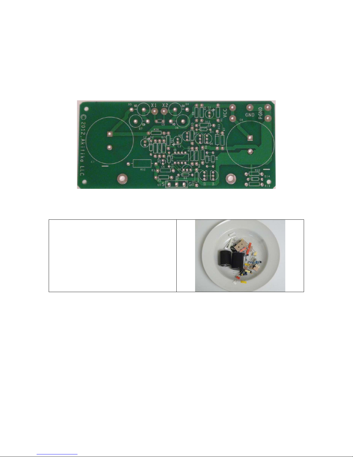
The are power supply PCB is shown in Figure 1.
Figure 1-Component side of power supply PCB before loading
Begin y carefully emptying the contents of the envelope marked “GT-101 PSU Module”
into a road soup owl, as shown elow. In general, you’ll start with the components that
lay closest to the oard, working your way towards the taller components. You will:
1. Install the resistors (all ut one
power resistor, left for later)
2. Install the diodes
3. Install the capacitors
4. Install the integrated circuits.
5. Install the transistors
6. Install the pass transistor Q5 as you
mount the PCB to the heat sink.
Component Order
You’ll notice that the component designations in the directions don’t go exactly in order.
We have grouped them so that all components with the same value appear together. This
makes assem ly easier. You’ll find in the parts kit that similar parts, e.g. 3 1K resistors,
are typically (though not always) taped together.
Install the Resistors
In general, you install the resistors y placing the ody on silk screen side of the oard,
and the leads through the indicated holes. Bend the leads over on the ack of the oard to
keep the resistors from falling out until your solder them in place. Try to end the leads in
a direction that won’t lead to solder ridges etween traces that should remain
disconnected.

Page 7 of 44
Figure 2-Installing resistors
We recommend the following procedure:
1. Insert all the resistors of the same value, e.g. R2, R3 and R4.
2. Bend the leads as descri ed a ove.
3. Solder the leads on the ack of the oard.
4. Clip the leads.
Track your progress y placing a check-mark in the done column as you install each
resistor. Check resistor values with a meter, or y reading the color code
1
. Orient the
resistor with the fat rown and on the right, then you can read oth the Color Code
column and the resistor from left to right.
¼ Watt, 1% resistors
Designation
Value Color code Done? ()
R2 1K Brown, Black, Black, Brown, Brown
R3 1K Brown, Black, Black, Brown, Brown
R4 1K Brown, Black, Black, Brown, Brown
R6 10K Brown, Black, Black, Red, Brown
R26 10K Brown, Black, Black, Red, Brown
R27 10K Brown, Black, Black, Red, Brown
R8 20K Red, Black, Black, Red, Brown
R9 20K Red, Black, Black, Red, Brown
R1 15K Brown, Green, Black, Red, Brown
R5 140K Brown, Yellow, Black, Orange, Brown
R7 5K76 Green, Violet, Blue, Brown, Brown
R10 26K1 Red, Blue, Brown, Red, Brown
R11
2
3K48 Orange, Yellow, Gray, Brown, Brown
R13 3M01 Orange, Black, Brown, Yellow, Brown
R22 165K Brown, Blue, Green, Orange, Brown
R23 100 Brown, Black, Black, Black, Brown
R24 95K3 White, Green, Orange, Red, Brown
R25 This location remains empty
We will defer installation of R12, a 0.1 Ohm power resistor, for a it later in the assem ly
process.
1
See “Appendix 1 - Resistor Color Code” on page 42 to see how to read resistor color codes.
2
See next page for location of R11. The R11 designation is missing from the silk-screen.

Page 8 of 44
Figure 3-R11 location (PCB s are missing the silk screen for R11)
Install the Diodes
Now install the diodes. Be careful to o serve the polarity markings on the diodes. You’ll
notice that one end of the diodes has a and. That and indicates the cathode of the diode.
Match the anded end of the diode with the anded end of the silk screen. The following
information should help you identify the diodes.
dentifying the glass body diodes
The glass ody diodes have the following identifying marks. If your vision is like mine,
you may need good light and a magnifying glass.
• 1N4148, D8-D11, has the num er 48 visi le
• BZX55B33B, D1 and D14, has the num er 33 visi le
• BZX79-B10, D2, has the num er 10 visi le
Also, typically when these diodes are packed, you can preliminarily identify the types
ecause:
• The 4 1N4148 diodes will typically e taped together
• The 2 BZX55B33B diodes will typically e taped together
• The 1 BZX79-B10 diode will e y itself

Page 9 of 44
D4-D7, opaque
lack plastic
package
D12, D13,
package type
DO-41, opaque
lack plastic
package
D1, D2, D8-
D11, D14,
package type
DO-35, glass
package
Keep track of the diodes as you install them using the following ta le. Remem er to
watch the polarity of the diodes, matching the anded end of the diode to the anded end
of the silk screen.
Designation Type, Package Description Done? ()
D1 BZX55B33, DO-35 33 Volt 2% zener diode
D14 BZX55B33, DO-35 33 Volt 2% zener diode
D2 BZX79-B10, DO-35 10 Volt 2% zener diode
D8 1N4148, DO-35 0.2 A, 100 PIV, switching
diode
D9 1N4148, DO-35 0.2 A, 100 PIV, switching
diode
D10 1N4148, DO-35 0.2 A, 100 PIV, switching
diode
D11 1N4148, DO-35 0.2 A, 100 PIV, switching
diode
D12 1N4004, DO-41 1A, 400 PIV, rectifier
diode
D13 1N4004, DO-41 1A, 400 PIV, rectifier
diode
Warning: Don’t cut the leads of D4-D7 until after the leads have een formed and the
diodes have een soldered into the PCB.

Page 10 of 44
Form the leads of D4-D7 as shown in Figure 4. Solder one lead of each diode while
attempting to keep the ody perpendicular to the plane of the oard. Ideally, the anodes
of D4-D7 should sit a out 1/8” to 1/16” off the oard.
Figure 4-Form the cathodes of D4-D7 as shown (banded end denotes cathode)
Designation Type, Package Description Done? ()
D4 6A4, R-6 6A, 400 PIV, rectifier
diode
D5 6A4, R-6 6A, 400 PIV, rectifier
diode
D6 6A4, R-6 6A, 400 PIV, rectifier
diode
D7 6A4, R-6 6A, 400 PIV, rectifier
diode
Install the Last Resistor
R12 should e air-mounted, with the ottom of its ody a out 1/8” a ove the PCB.
2 Watt, 5% resistor
Designation
Value Marking Done? ()
R12 0.1 0.1
Install the Small Capacitors
Now install the small capacitors:
C1, C2, and C3 are polarized, showing a minus sign (-) on the negative end of the
capacitor. Ma e sure that the minus sign faces away from the plus sign (+) mar ed on
the sil screen for each of the capacitors.
Designation Value Description Done? ()
C1 10 µF 100V electrolytic (polarized), cylindrical
shape
C2 10 µF 100V electrolytic (polarized), cylindrical
shape
C3 10 µF 100V electrolytic (polarized), cylindrical
shape
C4 100 nF 50V, Z5U, +/- 20%, marked 104
C5 10 nF 400V, film, 20%, ox shaped
Table of contents
Other AkitikA Amplifier manuals

AkitikA
AkitikA VC102 User manual

AkitikA
AkitikA GT-104 User manual

AkitikA
AkitikA PR-101 User manual

AkitikA
AkitikA PR-102 User manual

AkitikA
AkitikA GT-108 User manual

AkitikA
AkitikA PR-101 User manual

AkitikA
AkitikA GT-102 User manual

AkitikA
AkitikA PAT-4 User manual

AkitikA
AkitikA PR-101 User manual

AkitikA
AkitikA GT100 User manual

AkitikA
AkitikA PR-102 User manual

AkitikA
AkitikA GT-104 User manual

AkitikA
AkitikA EE-101 User manual

AkitikA
AkitikA PR-101 User manual

AkitikA
AkitikA PR-101NR User manual

AkitikA
AkitikA DYNACO STEREO 120 User manual

AkitikA
AkitikA PR-101 User manual

AkitikA
AkitikA PR102NR User manual

AkitikA
AkitikA PAT5RCA User manual

AkitikA
AkitikA PR-101NR User manual


